

 Authorized Dealer


With the continuous development and growth of the fast charger market, even giant enterprise like NOKIA have joined in to get a share of the pie.
Today, we got a Nokia 65W GaN fast charger P6308,It is equipped with three 2C1A USB ports and supports 65W PD fast charging, Huawei 22.5W SCP fast charging, etc. The selling points are portability and simultaneous charging of multiple devices. Let’s take it apart to see its internal components
- Product Appearance
The charger adopts a PC flame-retardant white shell, with a matte and glossy color design on the waist, rounded corners with a simple overall style.
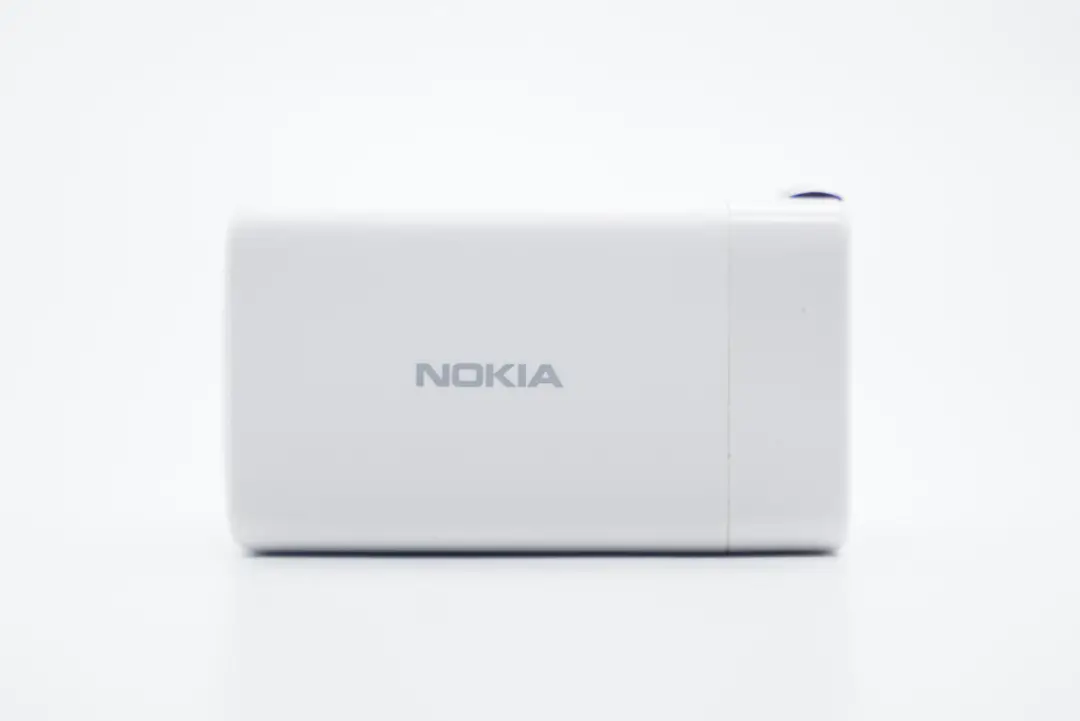
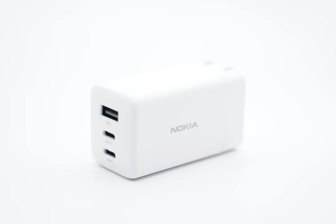
The NOKIA brand logo is printed on the side of the charger
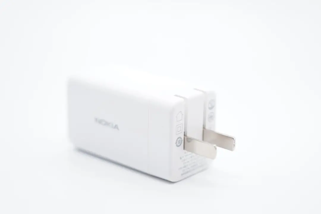
It is equipped with foldable national standard prongs which is easy to carry around
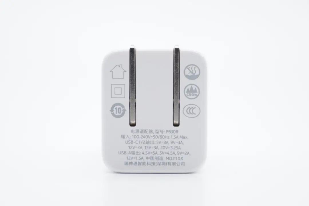
The Charger parameters are printed on the input shell.
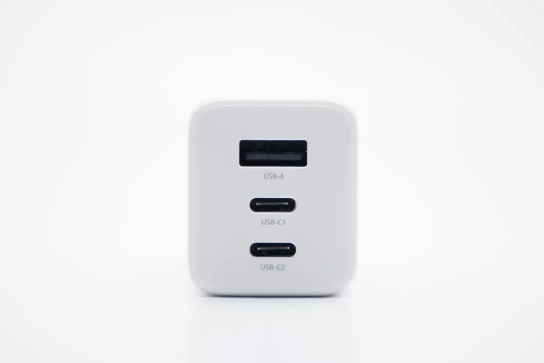
There are three Black USB ports on the top
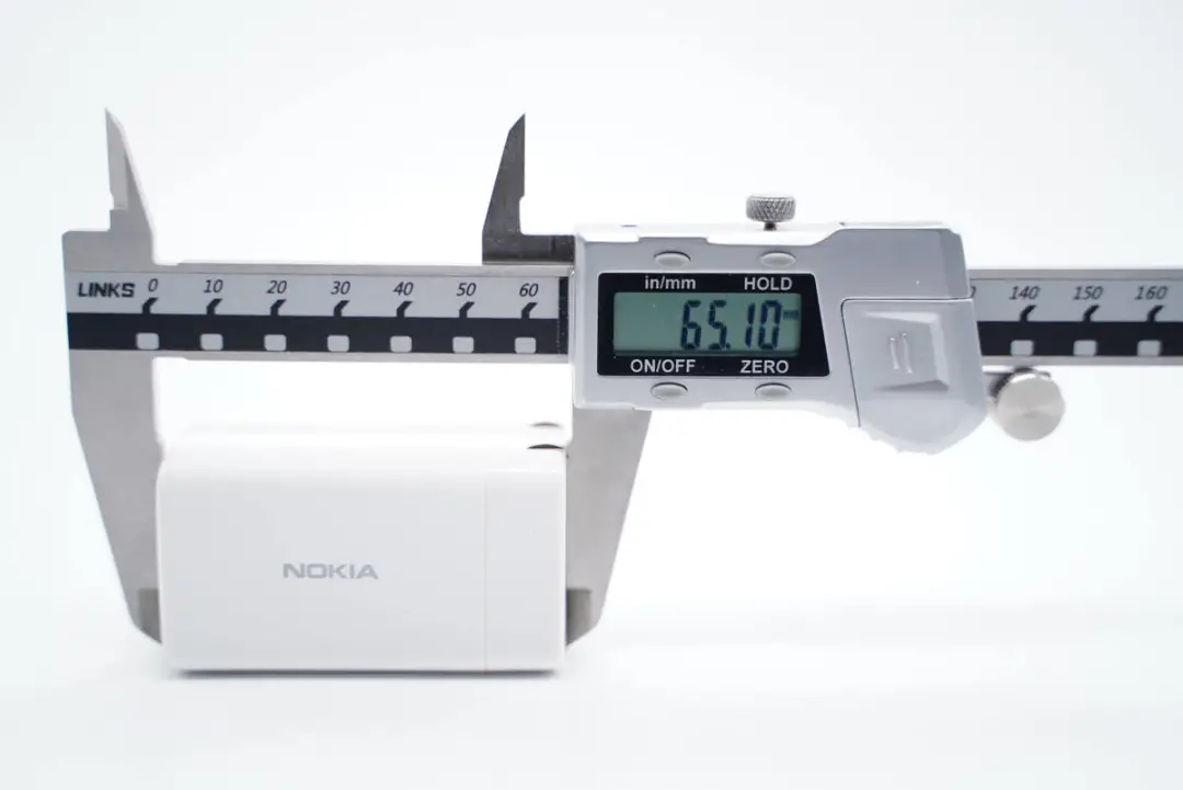
The height of the charger is 65.1mm.
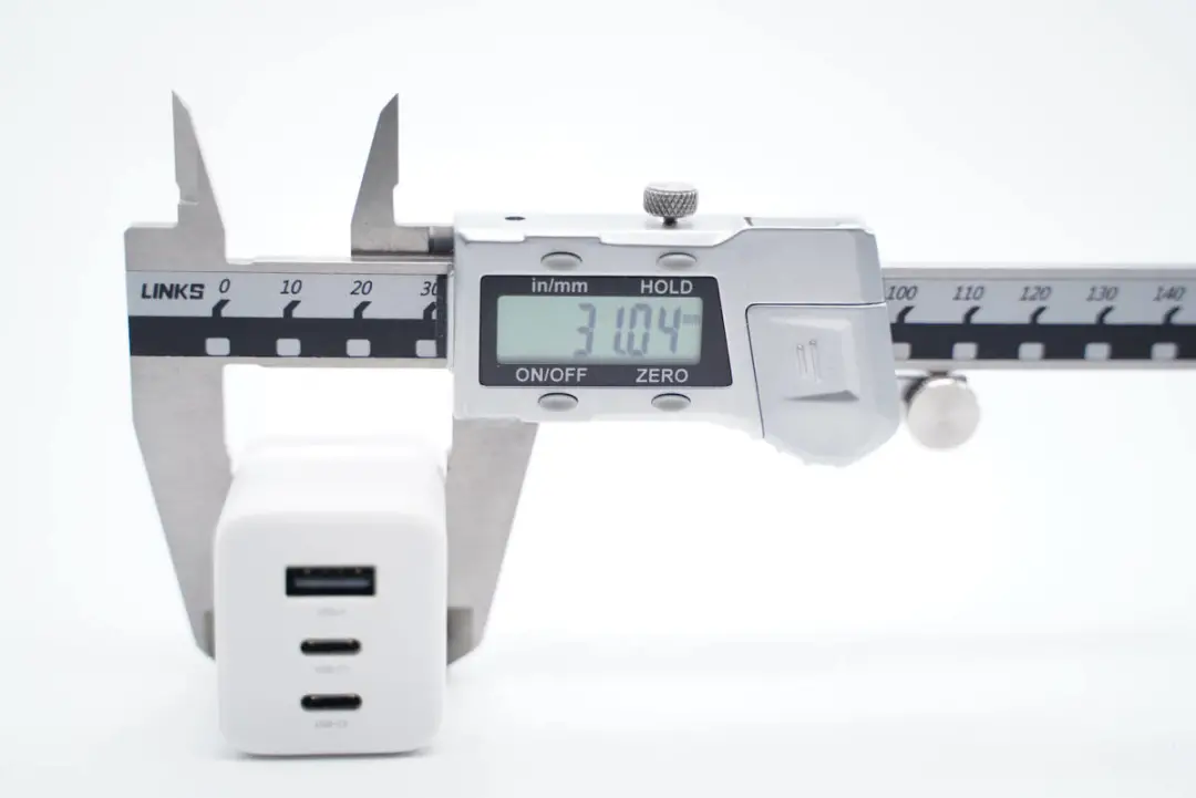
The width is 31.04mm.
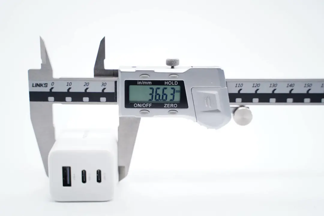
The thickness is 36.37mm. The charger volume is approximately 73.5cm ³ and the power density is 0.88W/cm ³
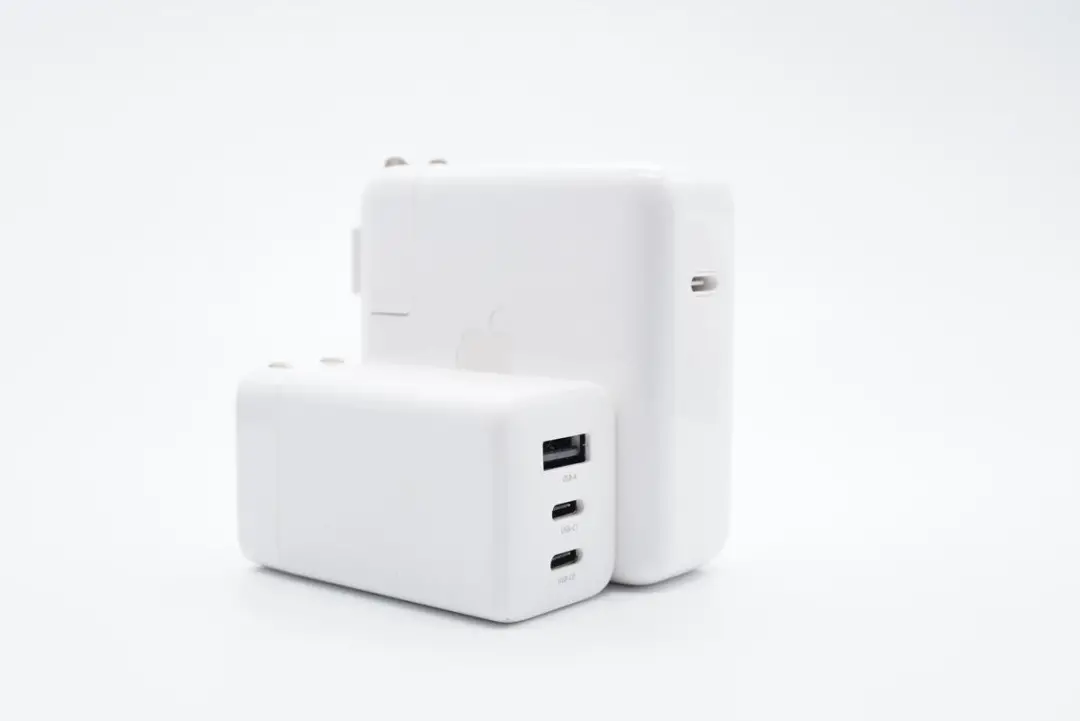
It is obviously smaller than the Apple 61W charger.
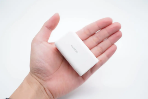
This is what it looks like in the hand.
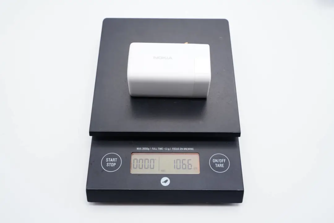
The Weight is about 107g

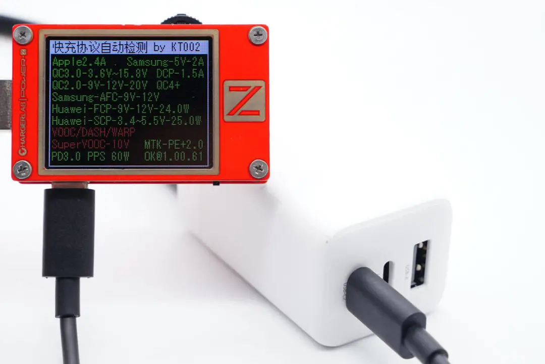
The ChargerLAB POWER-Z KT002 shows the USB-C1 port supports Apple 2.4A, Samsung 5V2A, DCP protocols, as well as QC2.0/3.0, FCP, SCP, PE2.0, PD3.0, and PPS fast charging protocols.
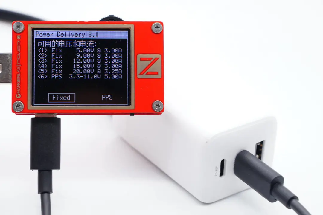
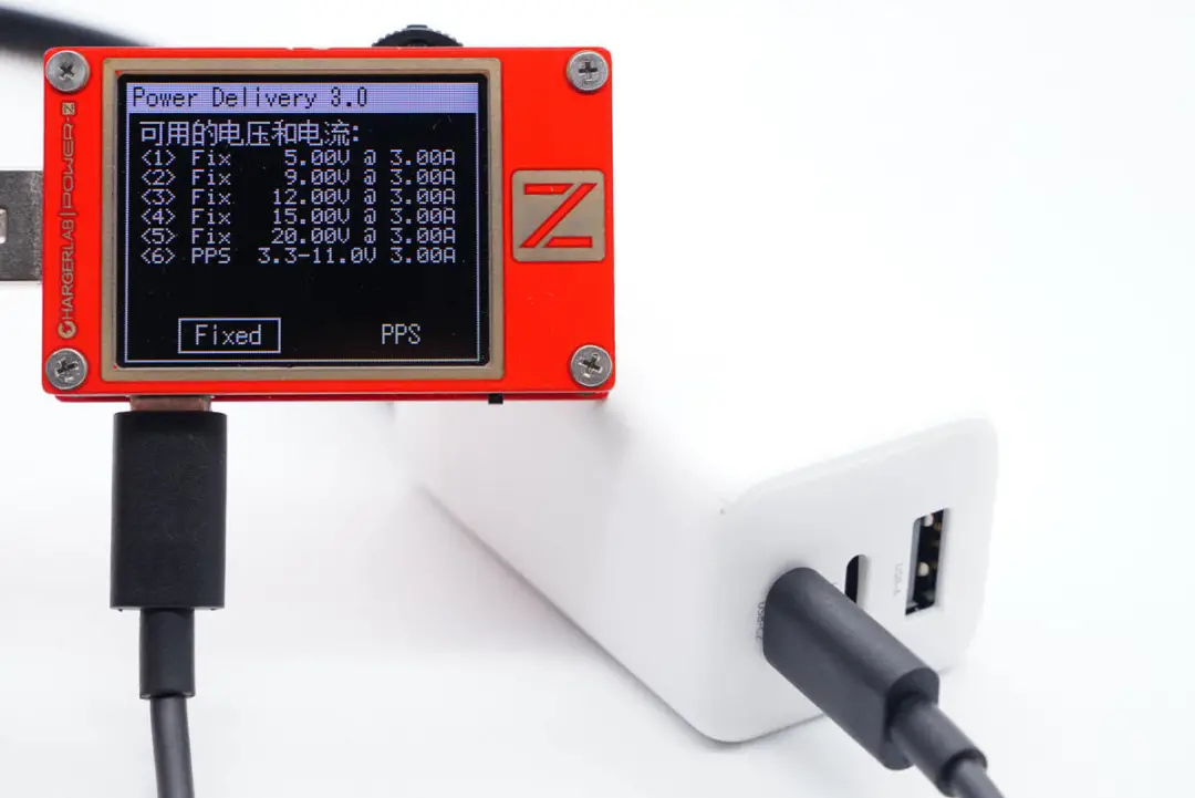
And the C1 port has five fixed PDOS of 5V3A, 9V3A, 12V3A, 15V3A, 20V3.25A, and a set of PPS 3.3-11V5A.
And the C2 port supports QC2.0/3.0, AFC, FCP, SCP, PE2.0, PD3.0, and PPS fast charging protocols.
The PDO message shows the C2 port also has five sets of fixed voltage levels : 5V3A, 9V3A, 12V3A, 15V3A, 20V3.25A, and a set of PPS voltage levels 3.3-11 V3A.
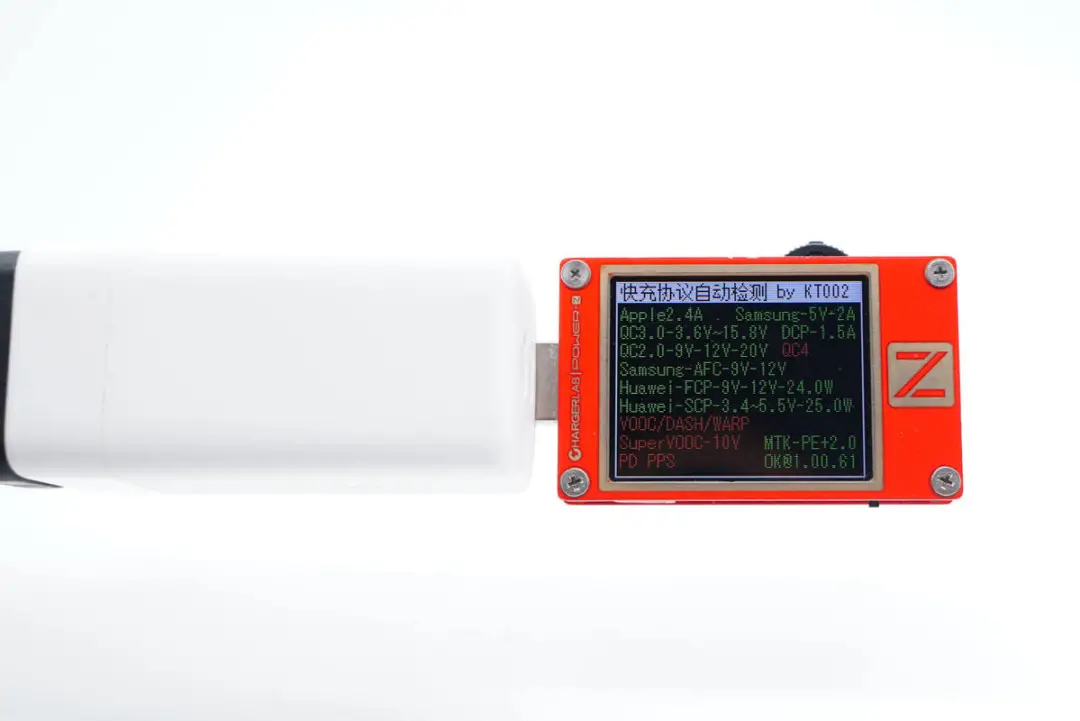
Finally, the USB-A port supports QC2.0/3.0, AFC, FCP, SCP, and PE2.0 fast charging protocols.
2.Teardown
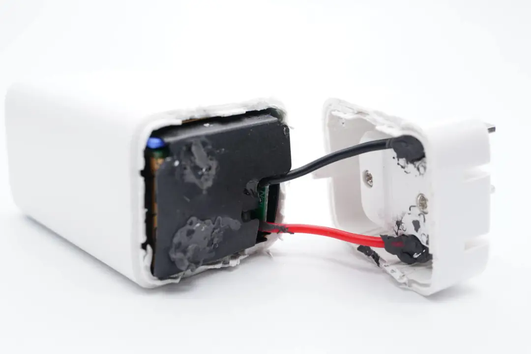
Remove the input cover,it shows an isolation board between the module and the pins.
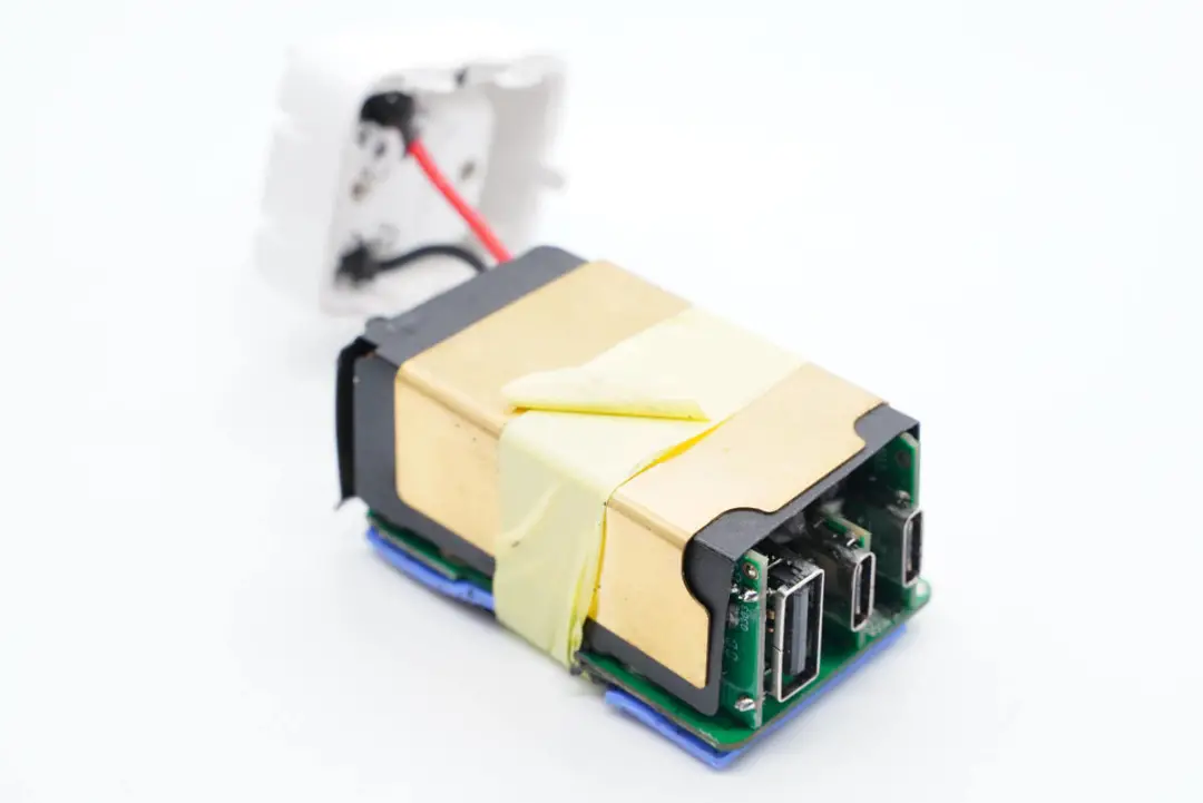
The entire module is covered by the brass heat sinks, and fixed with adhesive tape
The back of the main board also has a blue thermal pad to improve the heat dissipation, and the gaps between the front components are filled with thermal adhesive.
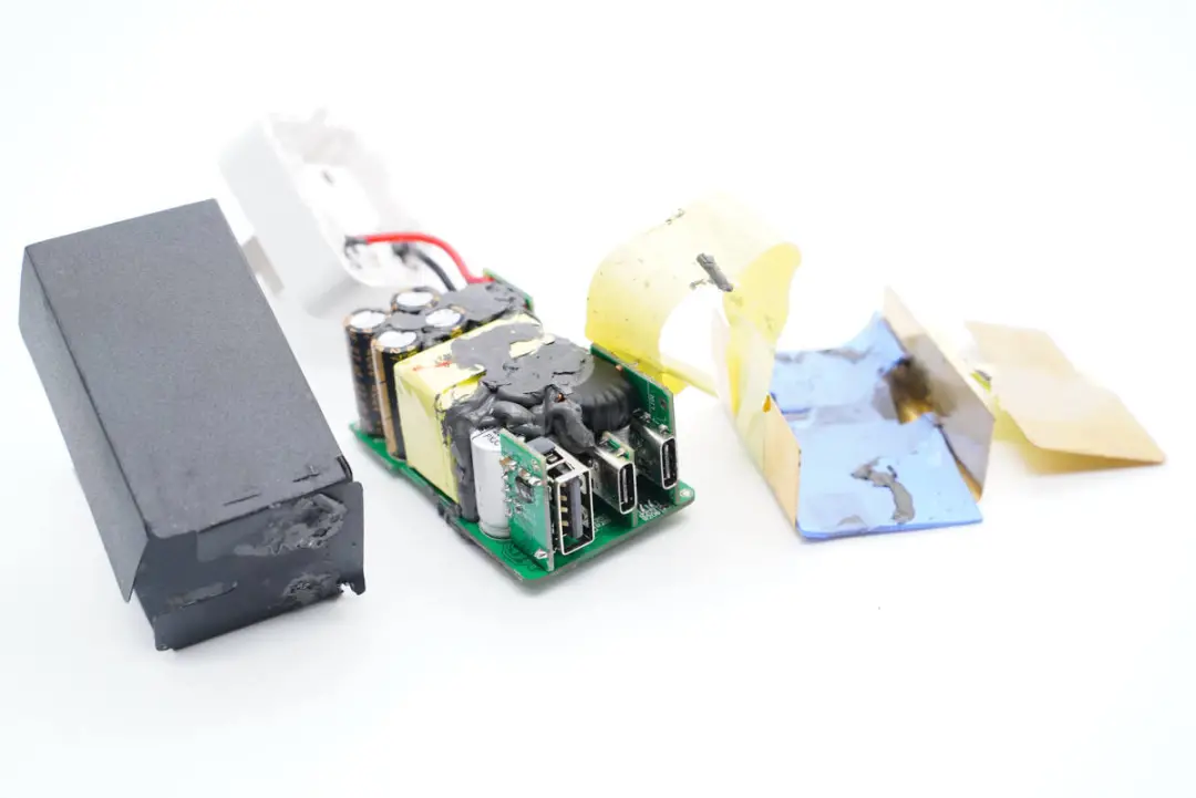
The front of the PCB board,the components adopt a classic three-stage layout, with a clear structure.
The back of the main board,It is equipped with a switching power supply and a DC-DC circuit.
ChargerLAB found it adopts a high-frequency QR switching power supply architecture, with two DC-DC secondary buck outputs, and power is intelligently distributed through the MCU.
Next,take a look at each components,starting from the input end.
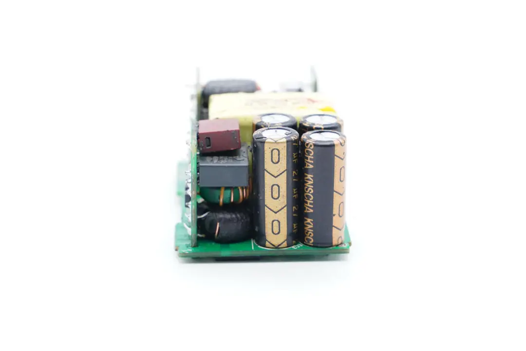
The input terminals, welding small board on the left, and four high-voltage filter electrolytic capacitors on the right.
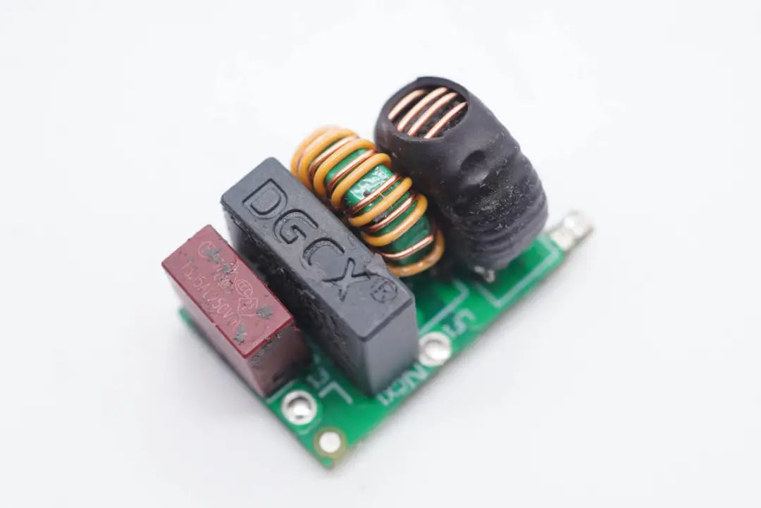
The small PCB board is equipped with a time- delay fuse, safety X capacitor, common mode inductor, and filter inductor.
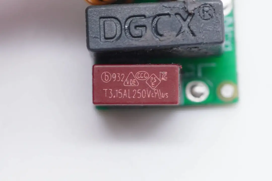
The specification of the time- delay fuse is 3.15A 250V.
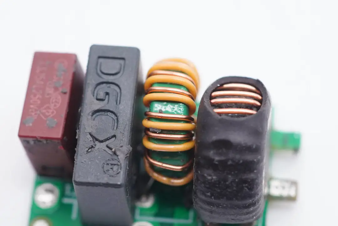
The safety X capacitor is from Chengxi Electronics, the common-mode inductor is double-wound to filter out EMI interference.
The Filter inductor is coated with an insulating tube.
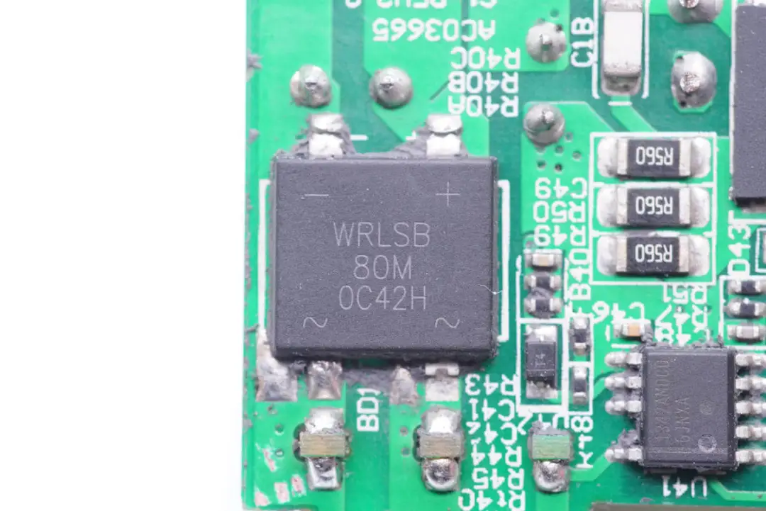
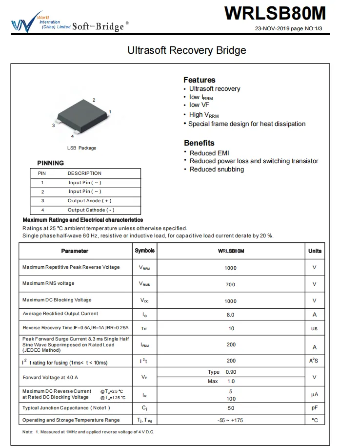
The input rectifier bridge WRLSB80M is from Shenzhen World Industrial Co., Ltd. The soft bridge has a relatively soft recovery curve and smooth turn-off characteristics, which can reduce the diode junction capacitance to achieve very little harmonic oscillation. The selected LSB package has good heat dissipation characteristics, which helps to improve the reliability of medium and large wattage adapters. A single unit can achieve 60W +
ChargerLAB found that MOMAX 100W 2A2C GaN fast charger, Nubia 1A1C 45W GaN fast charger, BULL 65W PD fast charging socket, Mcdodo 2C1A 65W GaN charger, HUWDER 65W GaN charger, OPPO 50W biscuit GaN fast charger, ROCK 65W GaN charger are using World soft recovery bridge. The product performance has been widely recognized by customers.
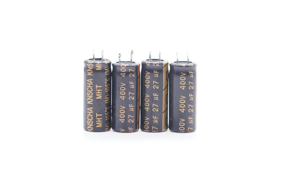
Four high-voltage filtering electrolytic capacitors are from KNSCHA 400V 27μF.

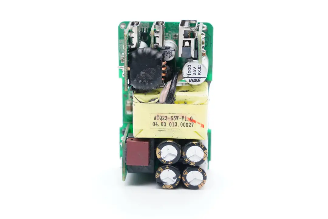
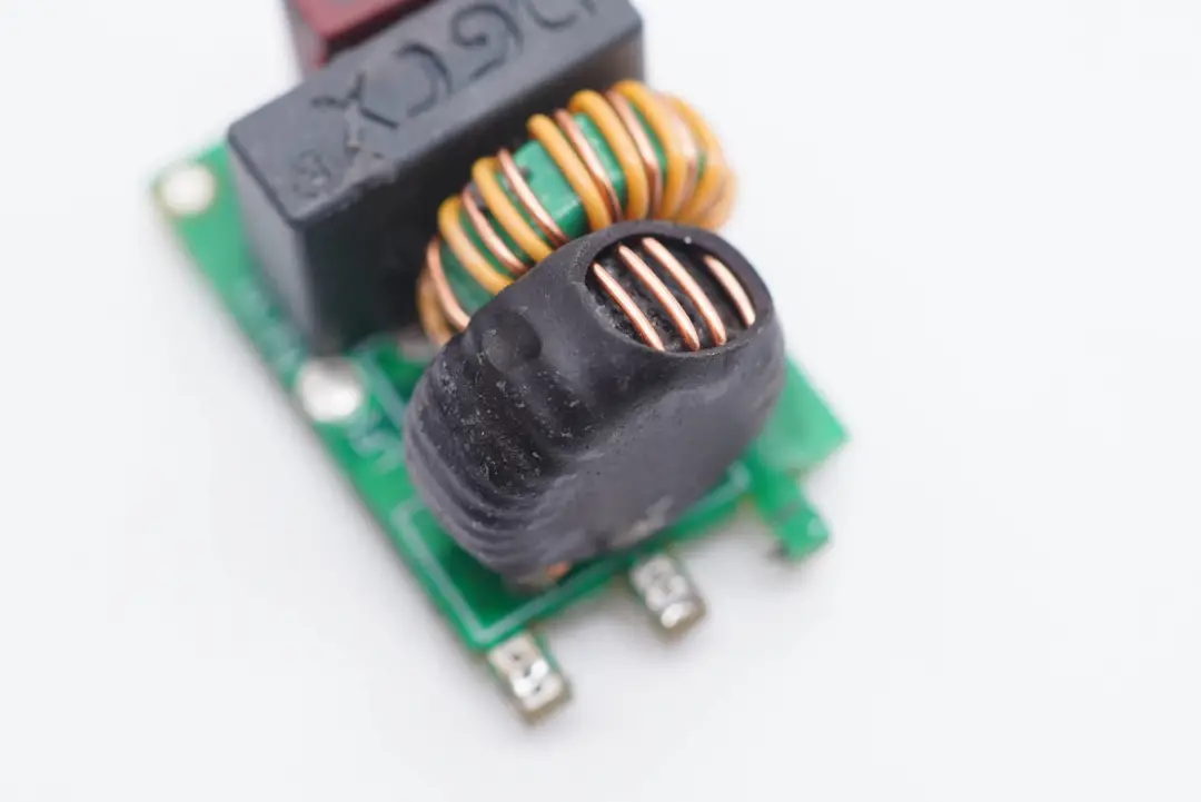
The module side, there is a transformer in the middle and an output filtering solid capacitor on the right.
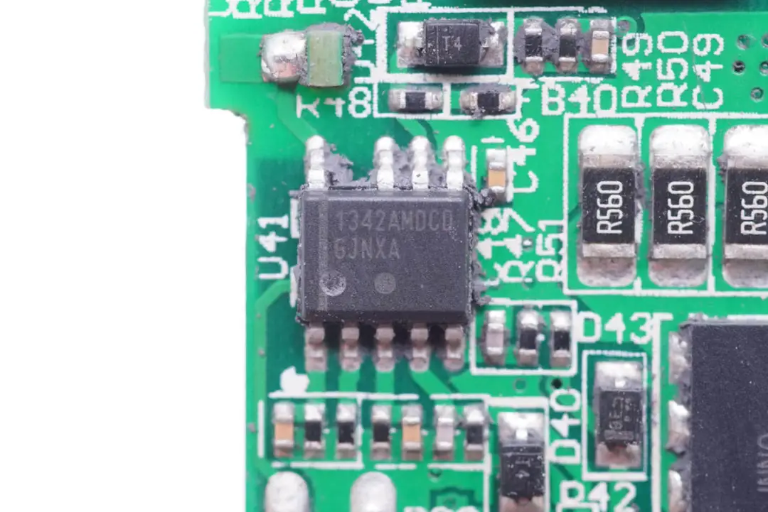
The main control chip of the switching power supply is ON Semiconductor NCP1342, It is a high-frequency flyback quasi-resonant primary PWM controller with built-in active X2 capacitor discharge, support for wide-range Vcc power supply, support for external thermistor overheating protection, and multiple comprehensive protection functions.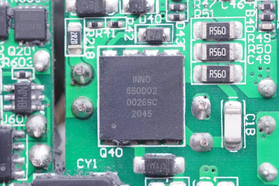
The high-voltage switch MOS tube uses the INN650D02 GaN power chip from Innoscience
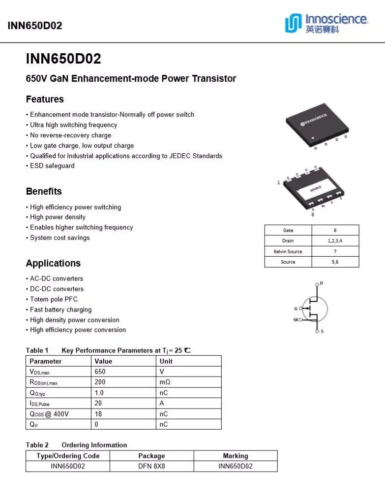
All specification of Innoscience INN650D02
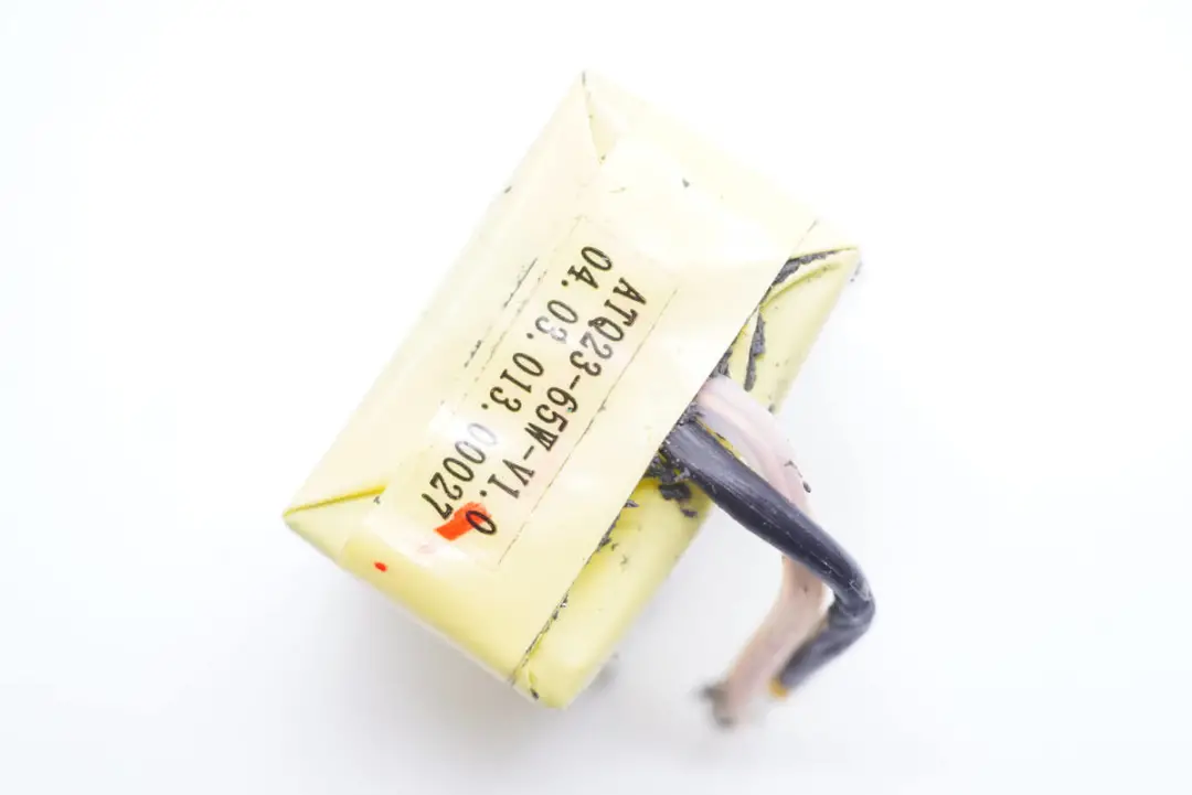
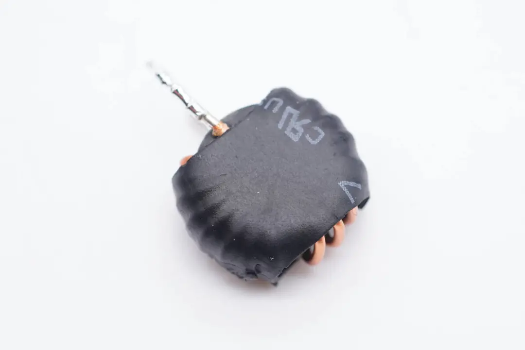
The ATQ23 transformer.
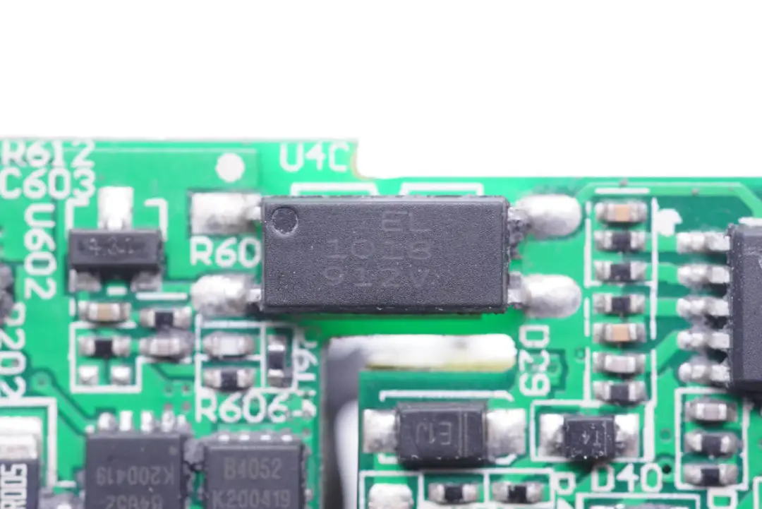
The EL 1018 optocouple, used for primary and secondary communication, feedback output voltage
The SMD Y capacitor is from Sichuan Teruixiang Technology Co.,Ltd.
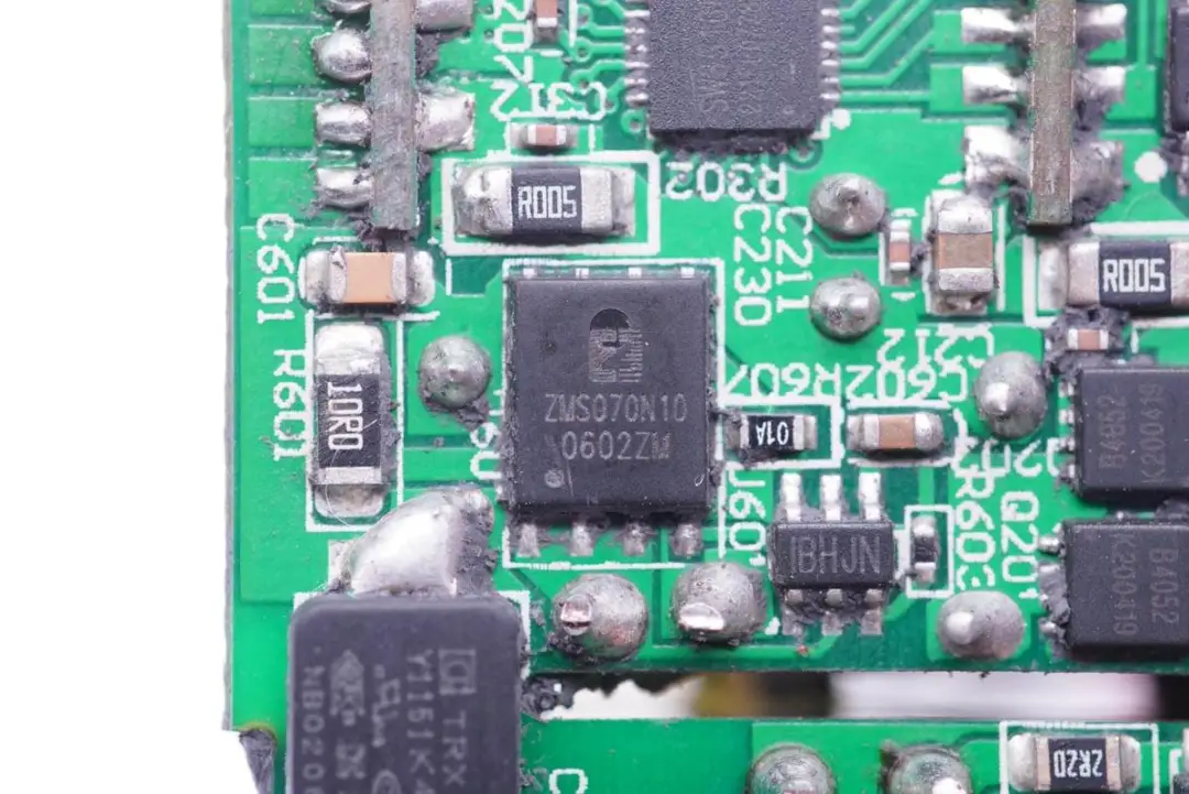
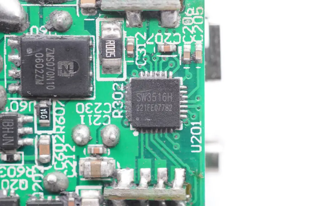
The synchronous rectifier adopts the Zhenmaojia ZMS070N10
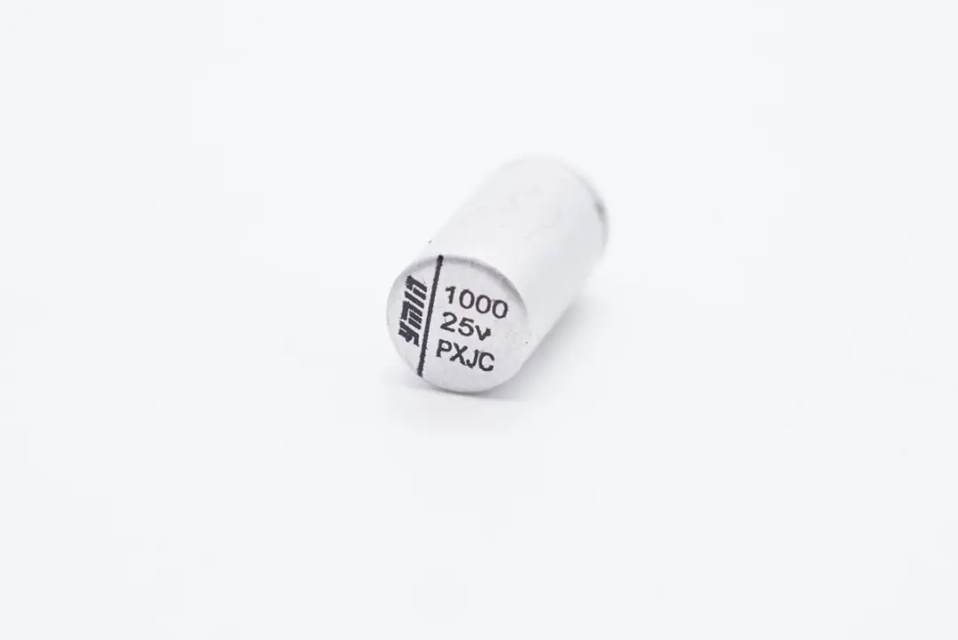
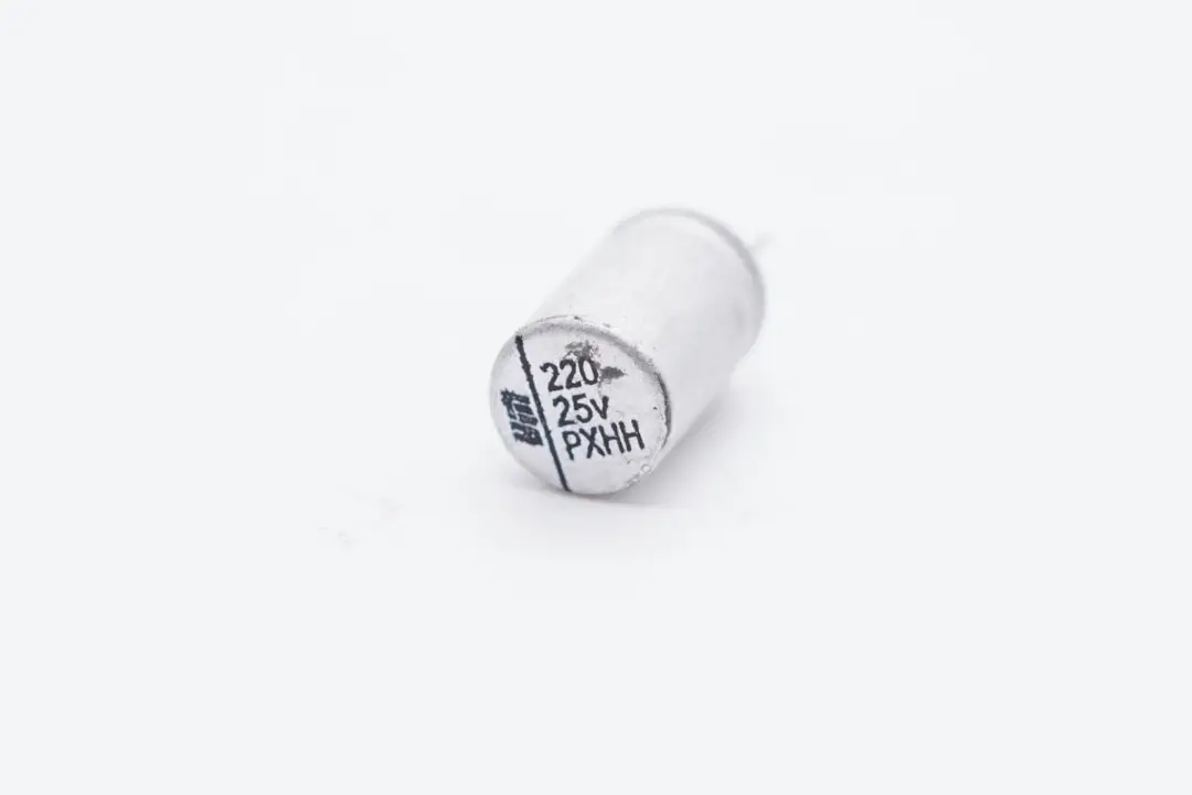
The output filter solid capacitor adopts the Yongming NPX series 25V 1000μF.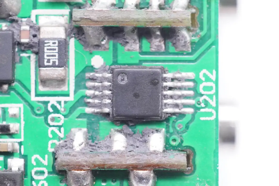
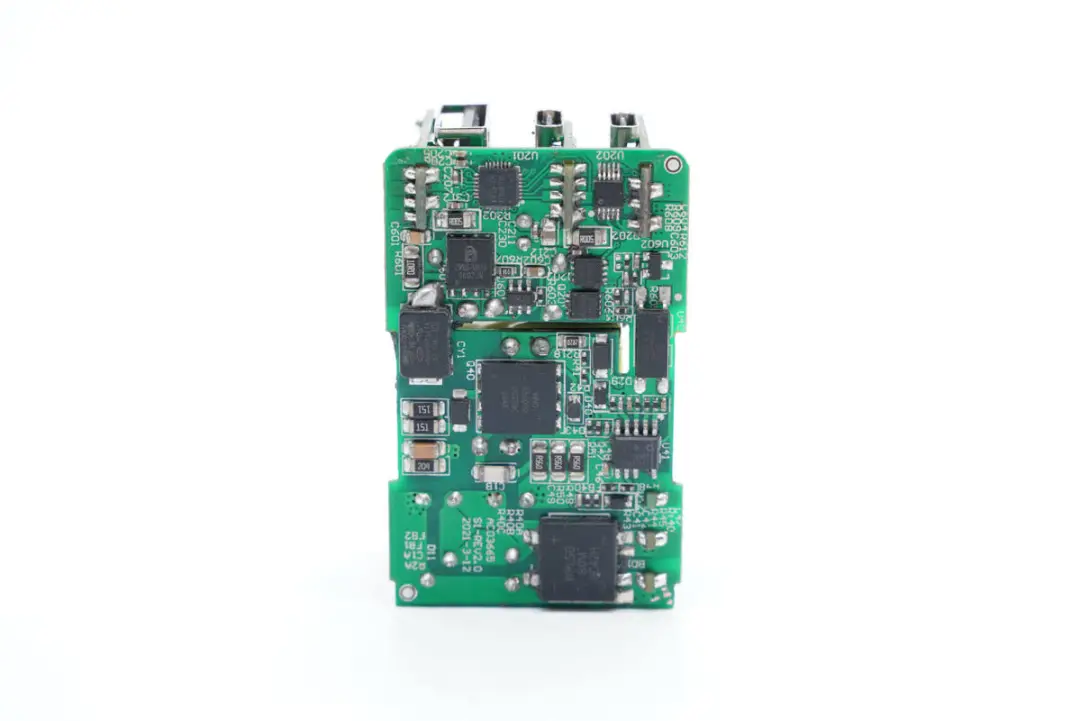
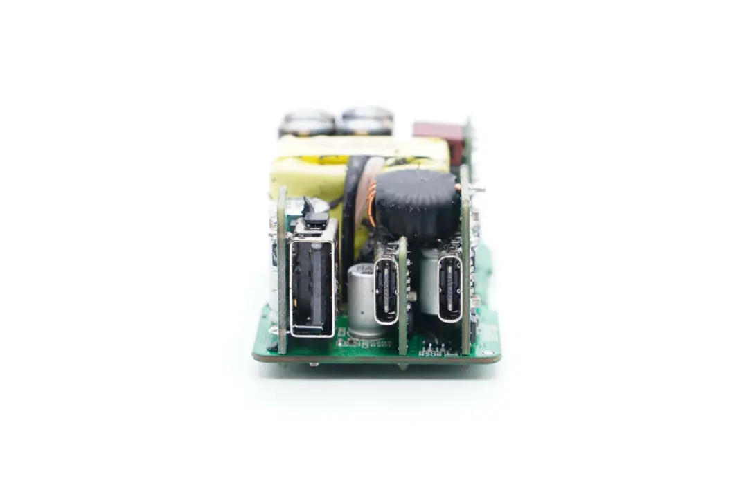
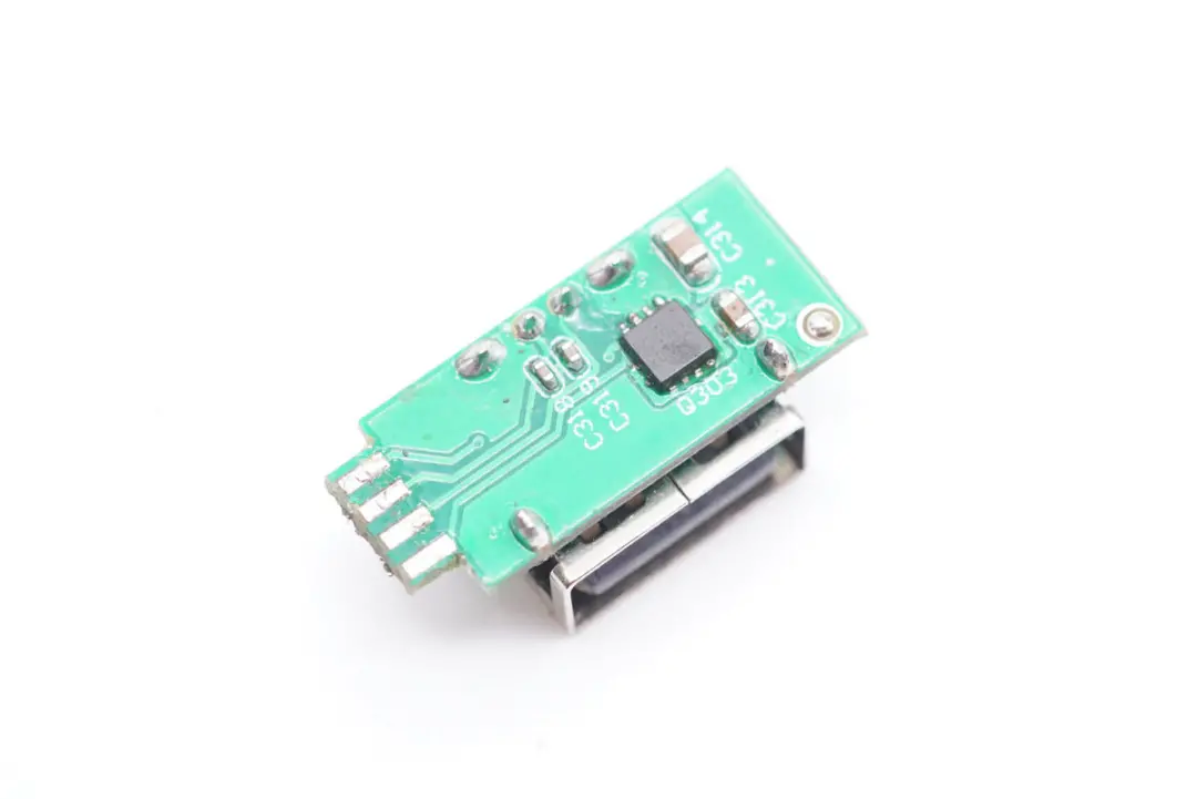
The three USB sockets are welded on the three PCB board respectively
The MCU is used for intelligent distribution of two channel DC-DC output power.
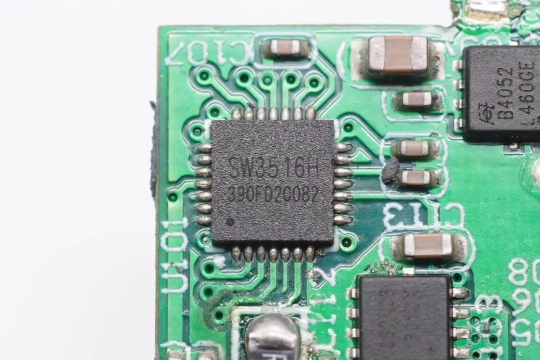
The BUCK master control chip of the USB-C1 and A is from ISMARTWARE SW3516H
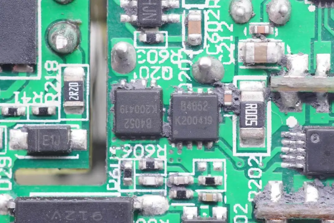
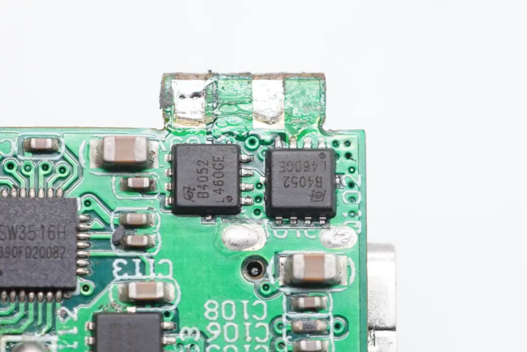
The FKBB4052 are used to synchronously rectify and buck of C1 and A port,with a voltage resistance of 40V and a resistance of 8.5mΩ.
The buck inductor is insulated by heat-shrinkable tubing.
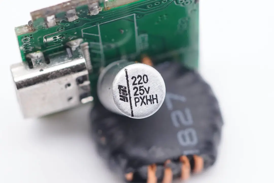
The filter solid capacitor is from Yongming NPX series 25V 220μF

The VBUS switch tube and USB-A socket are on this output PCB.
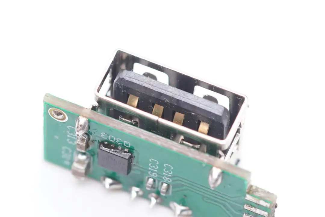
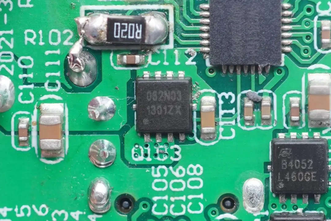
The MOS printing 062N03.
USB-A socket, via-hole welding.
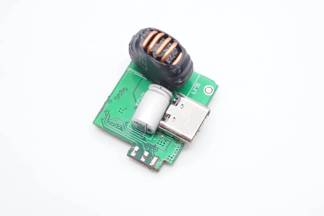
The same VBUS switch tube and USB-C1 socket are on this output PCB.
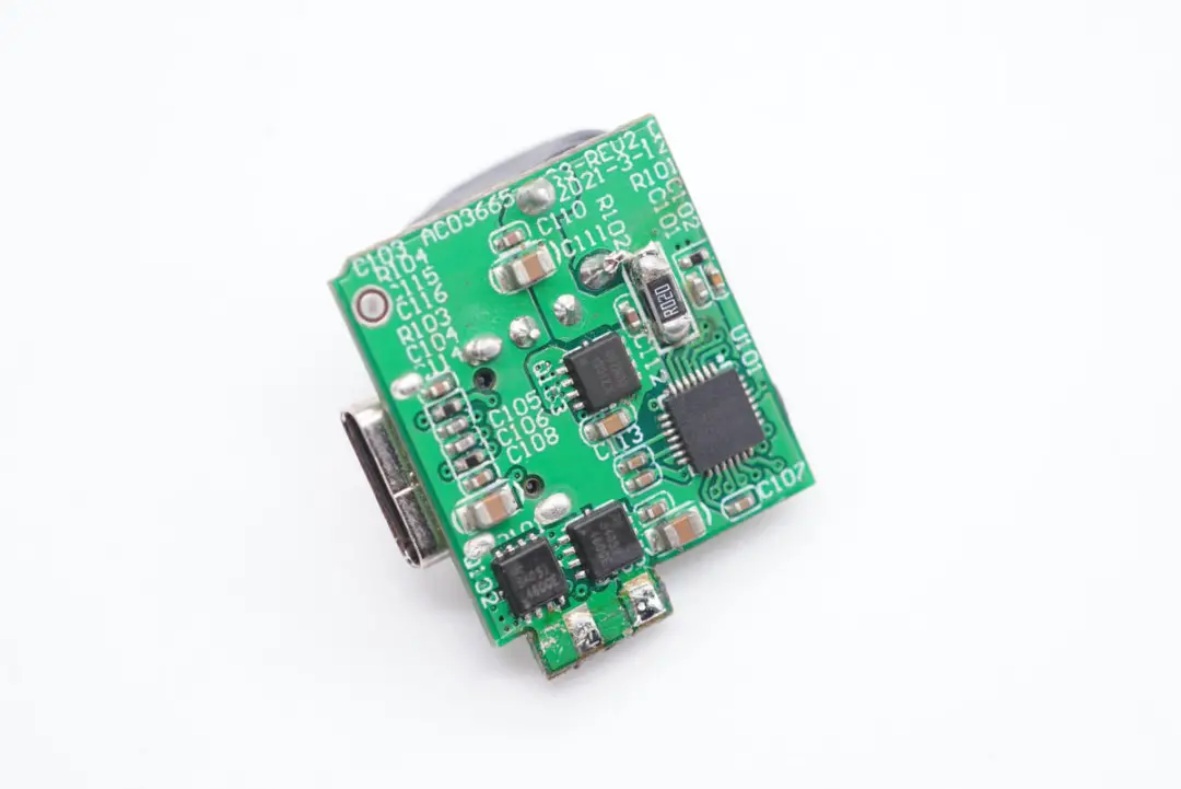
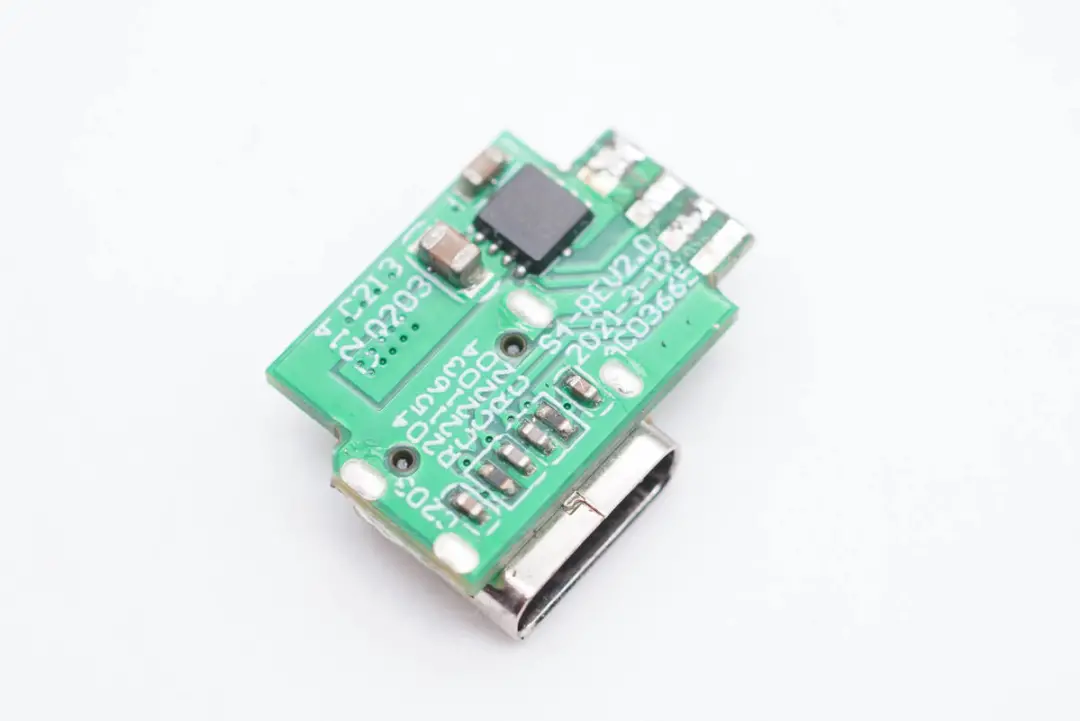
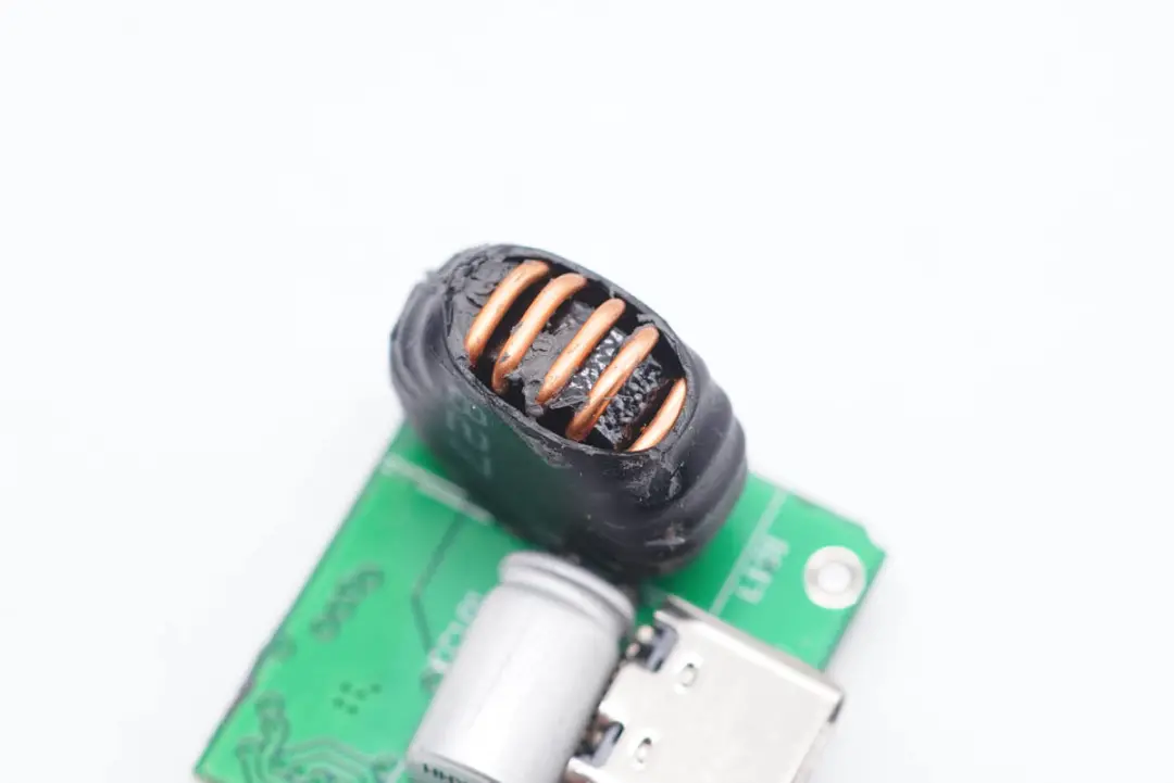
The front of the PCB board where the USB-C2 socket is located is equipped with a buck inductor and a filter capacitor.
The other side is equipped with a buck protocol IC and three MOSFETS
The BUCK protocol IC is also from Zhirong SW3516H.
The two external MOSFETs also from Dongyuan FKBB4052.
Buck inductor.
Yongming NPX series filter solid capacitor 25V 220μF.
Output VBUS switch tube with screen printing 062N03.
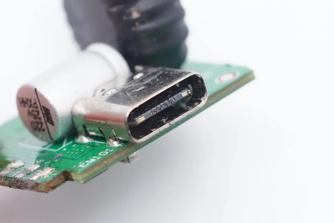
USB-C2 Socket
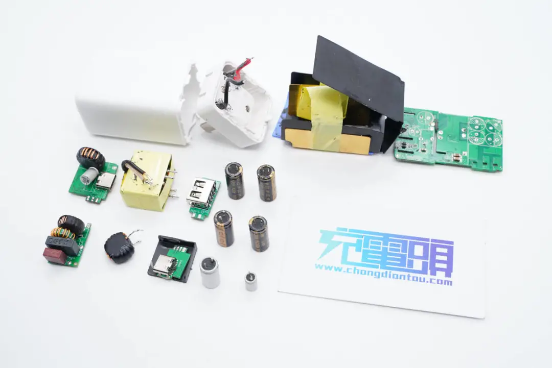
That’s all for the teardown
Summary of ChargerLAB
Nokia 65W GaN fast charger with a mainstream cylindrical body, folding pins, and a 2C1A interface. And the volume control is good with only 73.5cm ³, and a power density of 0.88W/cm ³. Compared with many three-port GaN fast chargers on the market, it performs quite well.
The ChargerLAB found the secondary side of the charger adopts a two-way DC-DC secondary buck output design, and both use the intelligent SW3516H solution. Thanks to the use of this chip, the equipped 2C1A interface is compatible with QC, AFC, FCP, SCP, PE2.0, PD3.0, and PPS all mainstream fast charging protocols, which can support fast charging of two devices such as laptops and mobile phones at the same time.