

 Authorized Dealer


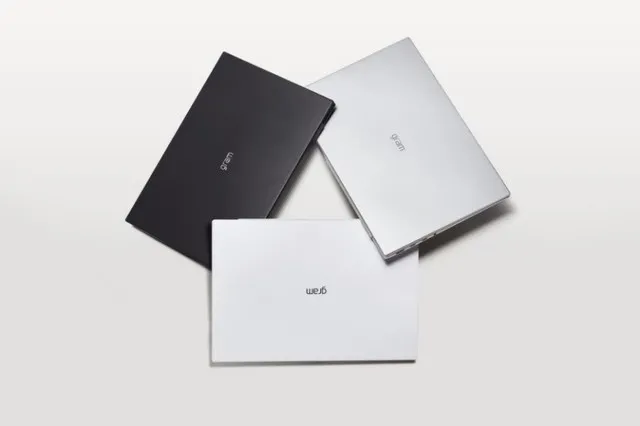
In 2021 years, LG Electronics launched the highly anticipated new LG Gram laptop at the first CES 2021 virtual online exhibition and won the CES 2021 award.
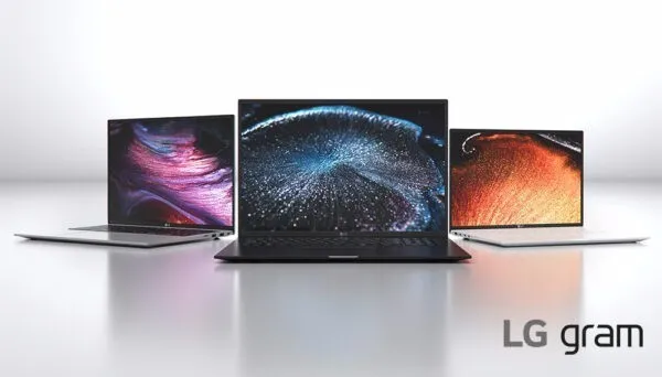
The new laptop is the thinnest 16-inch laptop on the market currently, with a total weight of only 1190g.
We got the standard power supply of this laptop today, It adopts a standard laptop adapter design (input 8-shaped, built-in output Type C), and the output supports PD/PPS fast charging, with a maximum output power of 65W.
The charger adopts an arc-shaped brick design to improve safety and achieve better heat dissipation. The user-friendly design makes it easy to hold without any pressure. Now let's take it apart to see the internal design.
- Product Appearance
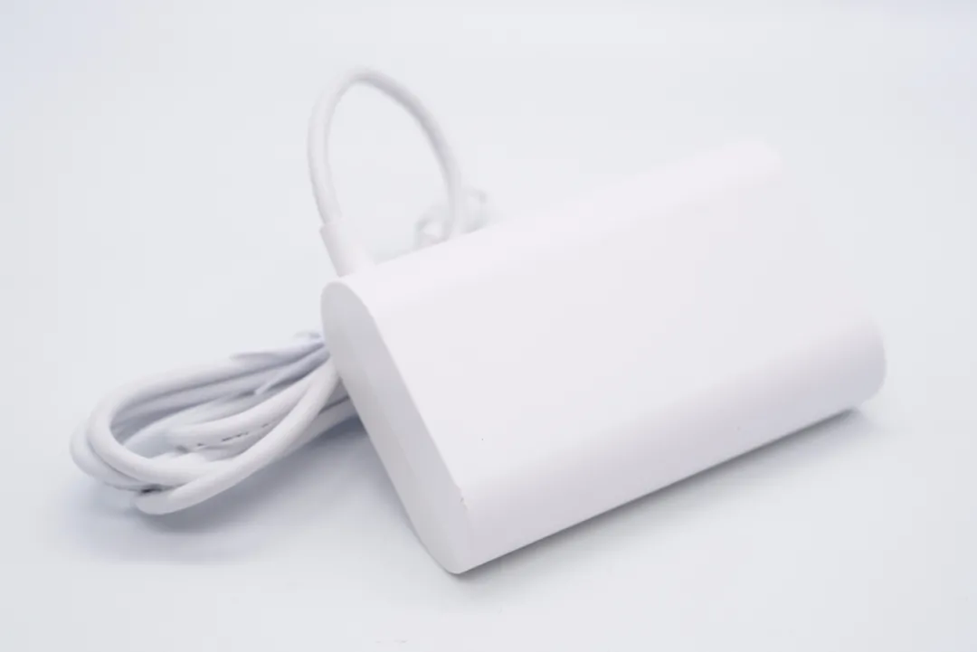
The LG 65W GaN charger with a standard laptop power adapter design, comes with a USB-C output cable, and has a frosted surface with curved edges on both sides.
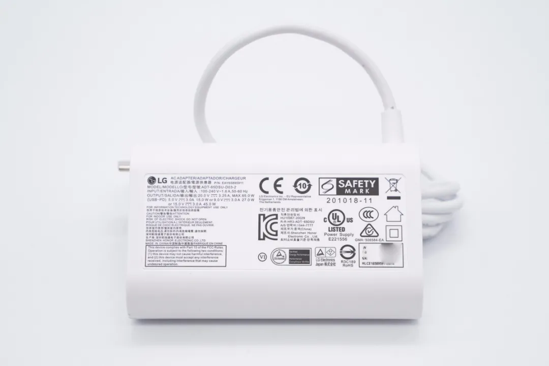
The parameters are labeled on the back of the charger
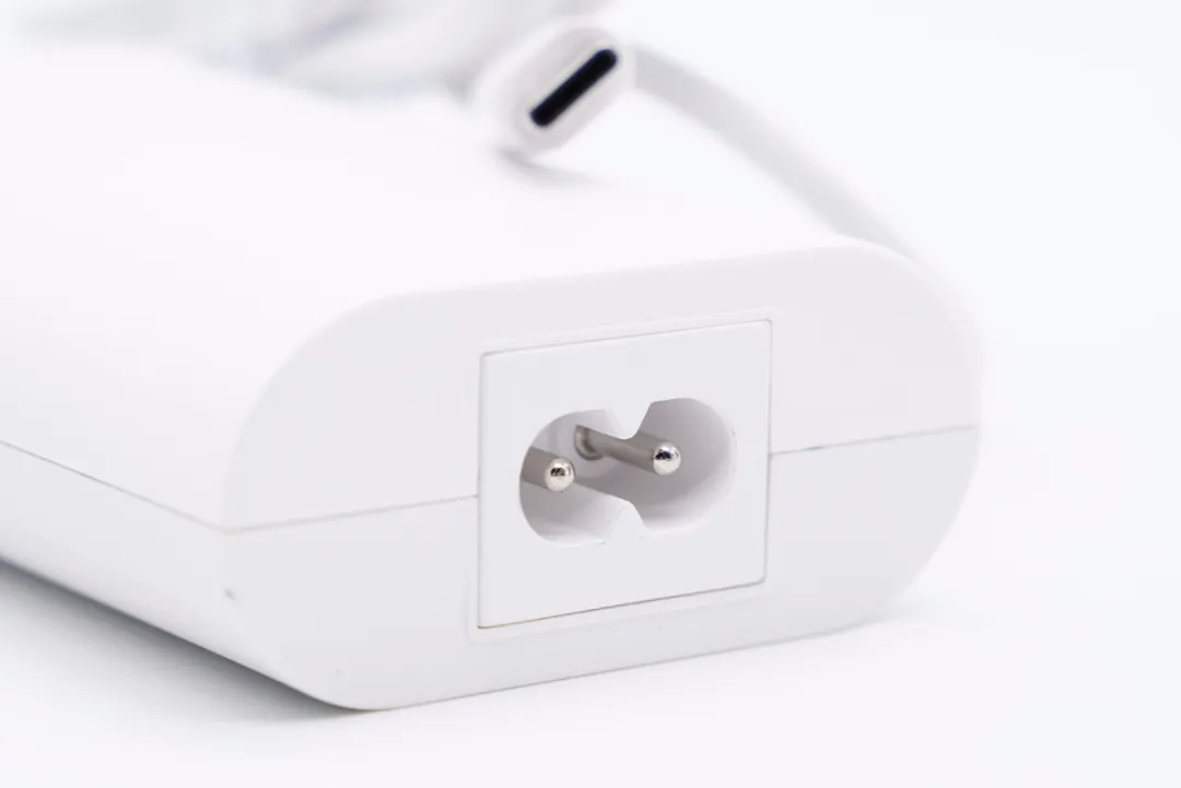
The charger adopts an 8-shaped input ports, which can replace the corresponding specification power cord according to different regions
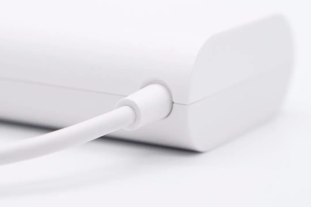
The output cable and the junction of the charger have undergone anti-bending treatment.
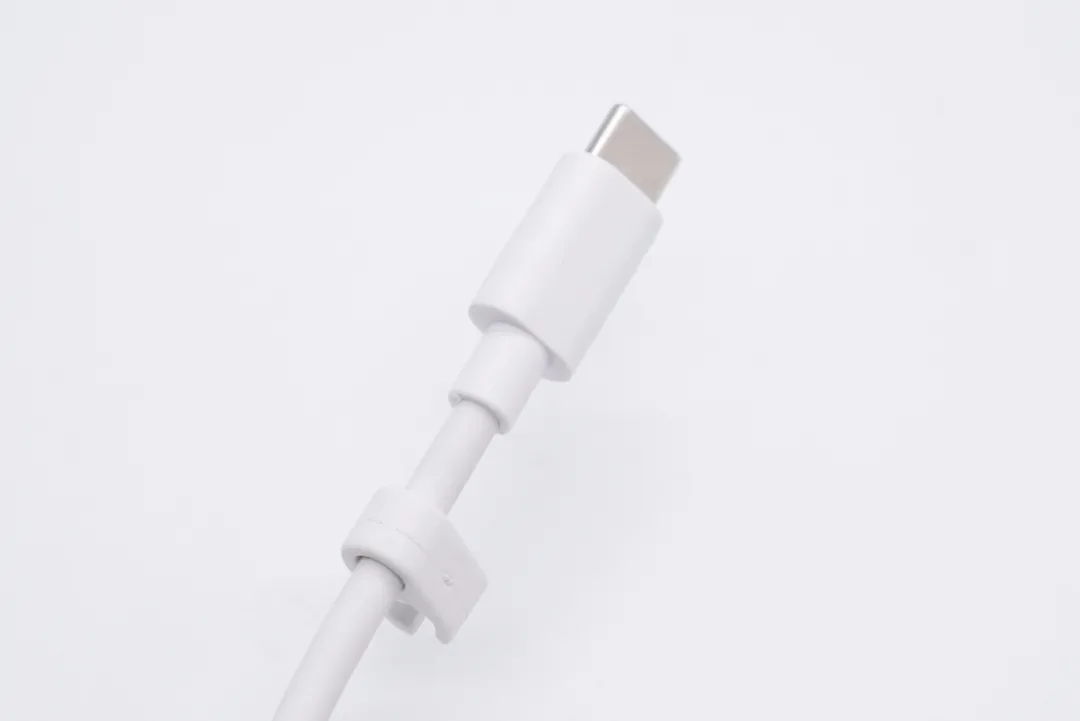
The other end of the cable is designed with a locking buckle for easy sorting.
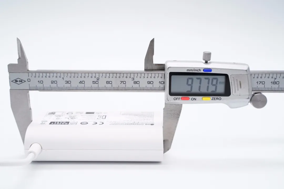
The length of the charger is 97.79mm.
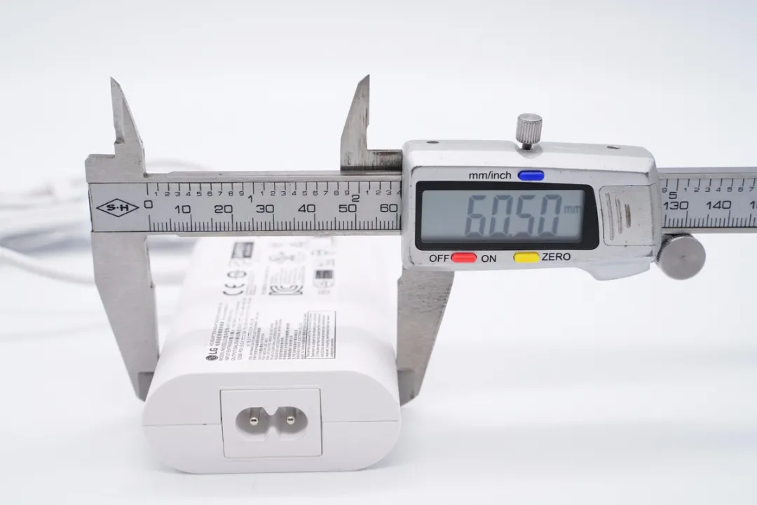
The maximum width is 60.5mm.

The thickness is 27.05mm.
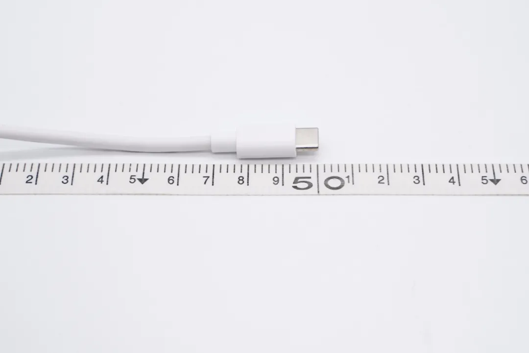
In addition, the built-in cable is about 1.5 meters long, which meets daily use.
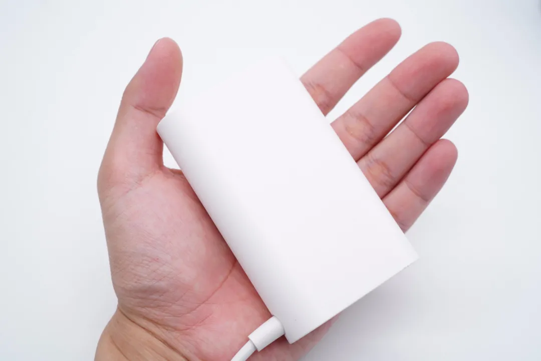
This is what it looks like in the hand.
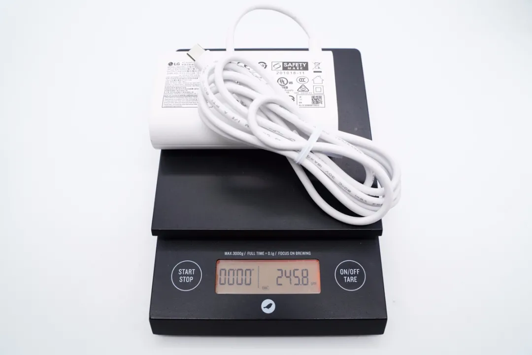
The total weight of the charger cable is about 246g.
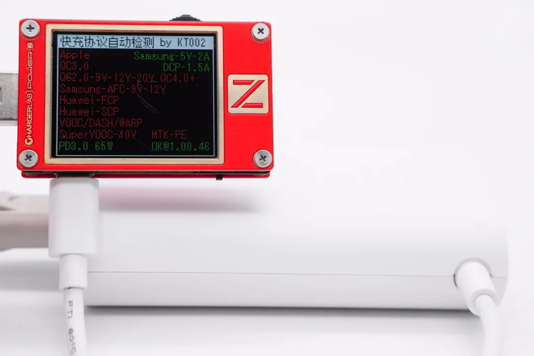
The ChargerLAB POWER-Z KT002 shows only supports the PD3.0 fast charging protocol.
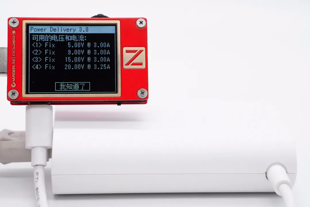
The PDO message shows it has four sets of fixed voltage levels : 5V3A, 9V3A, 15V3A, and 20V3.25A.
- Teardown
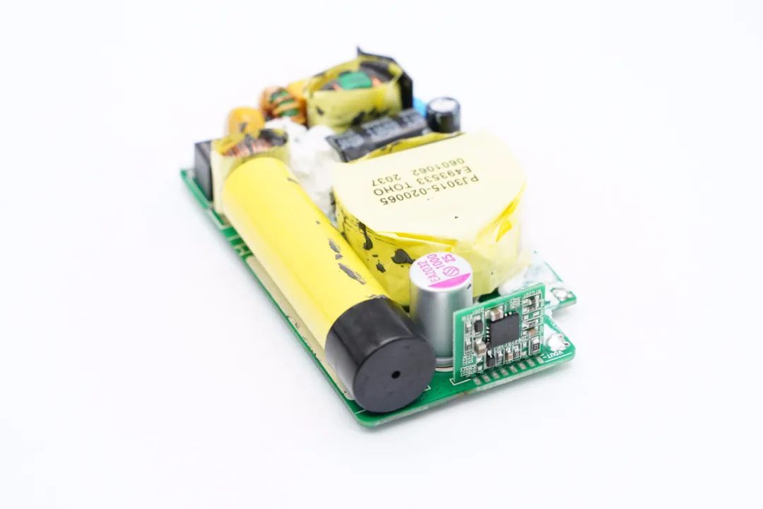
Remove the bottom cover. The PCBA module is covered by the copper heat sinks and filled with glue between the cover for better heat dissipation.
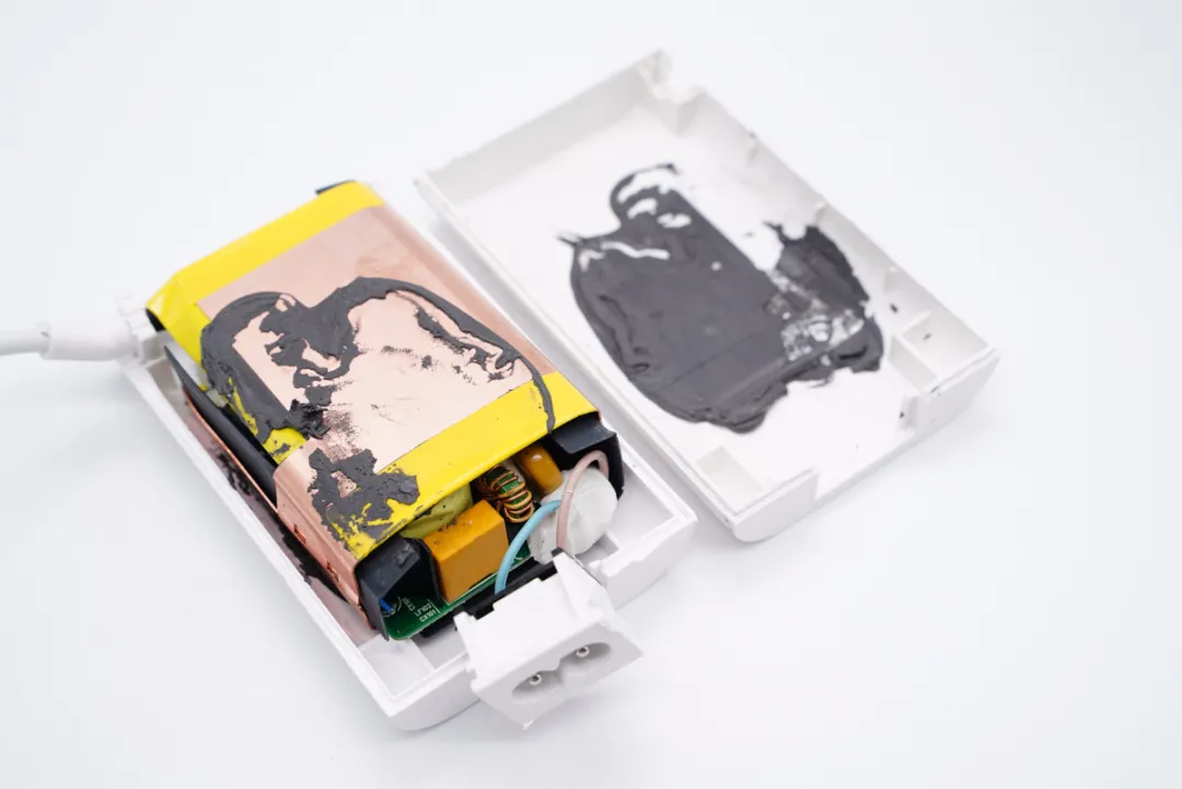
Paste insulating tape inside the heat sink, there is a insulation board between the heat sink and circuit board for isolation.
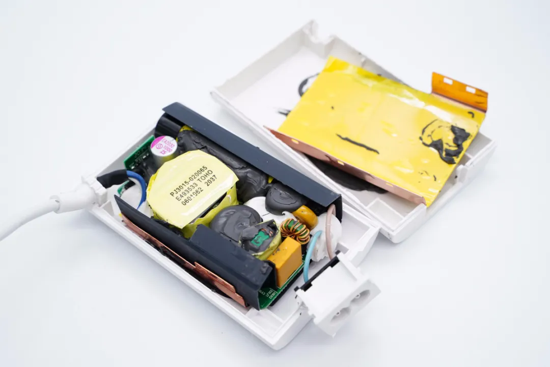
The output and input wires are insulated by gluing at the welding points.
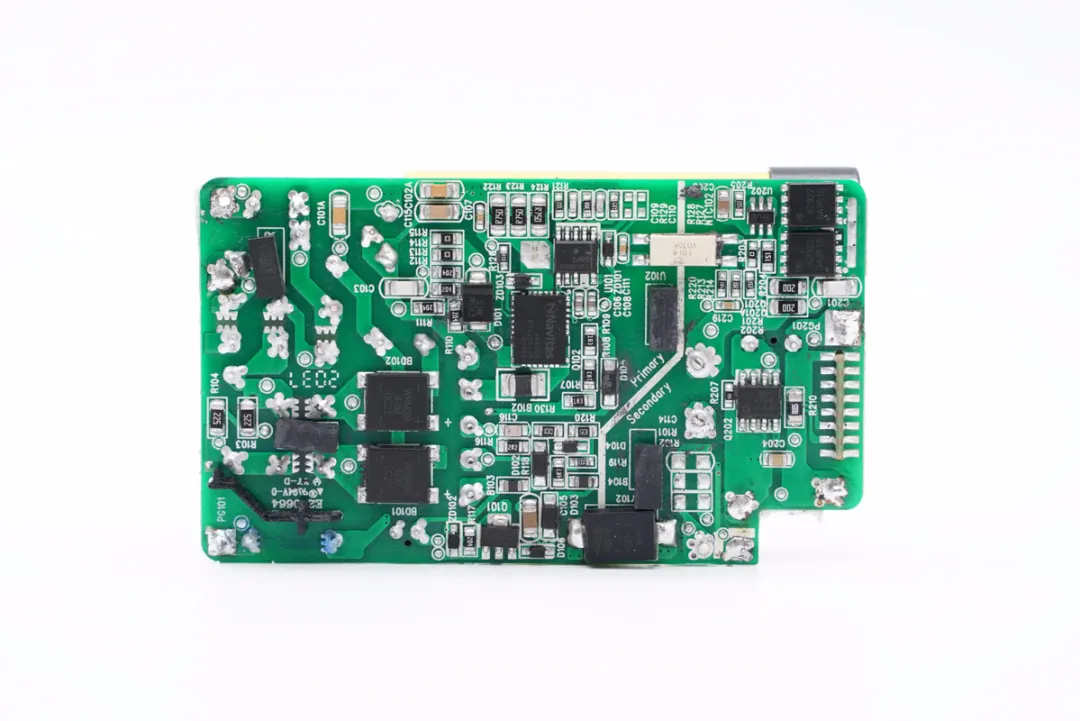
The front of the PCB board with Black and white glue for reinforce and conduct heat.
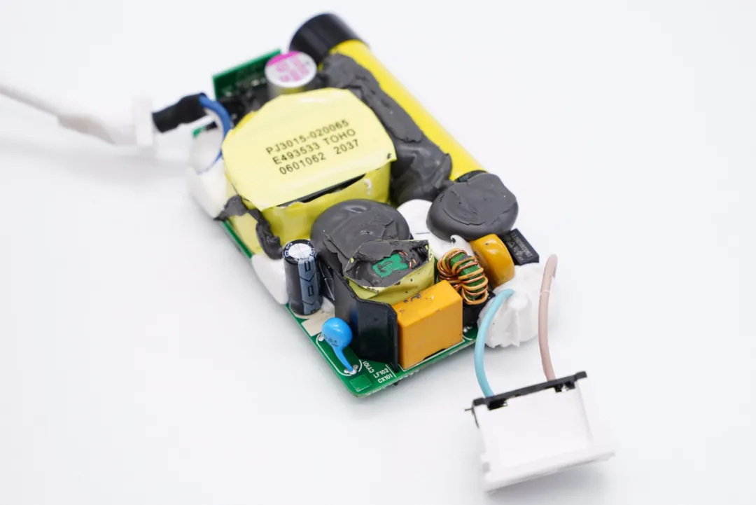
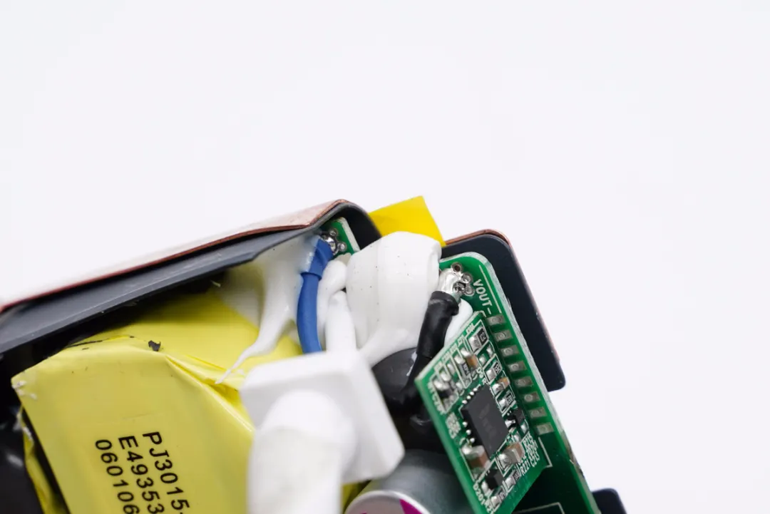
The front of PCB board, with a compact layout of components at the right input end and only one solid capacitor and protocol board at the left output end
The back of the PCB board is coated with a large amount of black silicone for the chip conduct heat.
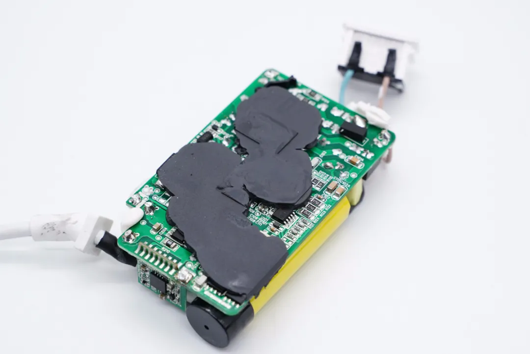
Clean up and find the multiple support pads on the back, with two rectifier bridges, a primary master control chip, a GaN power switch tube, a white optocoupler, a secondary controller, two synchronous rectifier tubes from left to right, and below with an output VBUS switch tube .
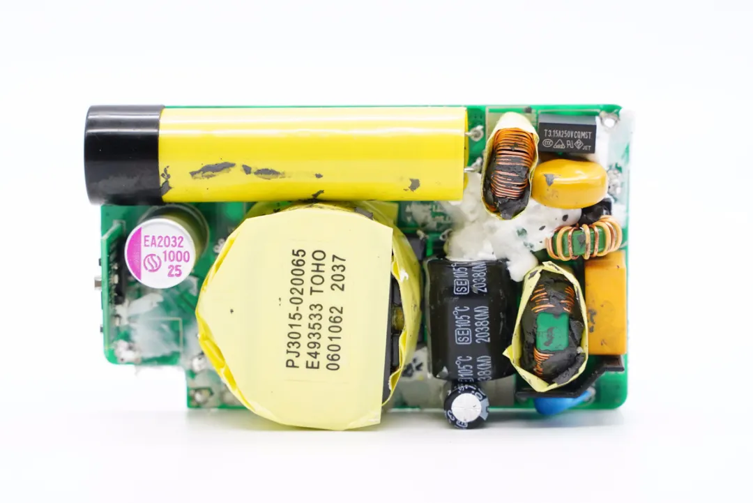
ChargerLAB found the LG 65W GaN fast charger uses a typical flyback switch power supply with a wide range of output, and the output voltage is controlled by a secondary protocol chip through optocoupler feedback. Now let's start with the input end to see each component.
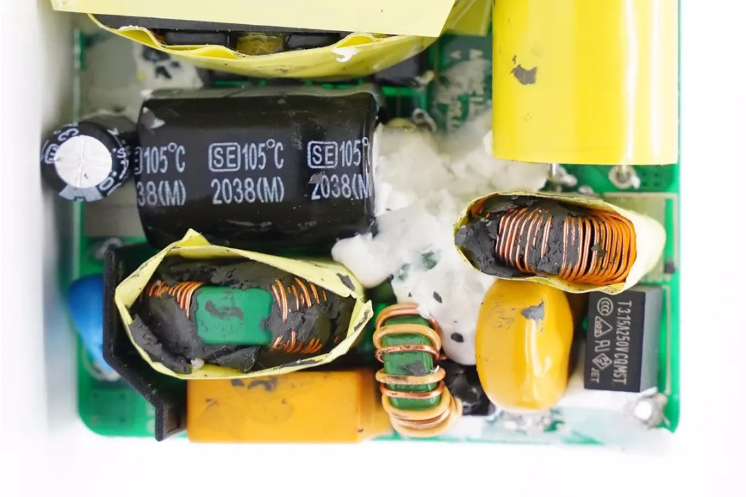
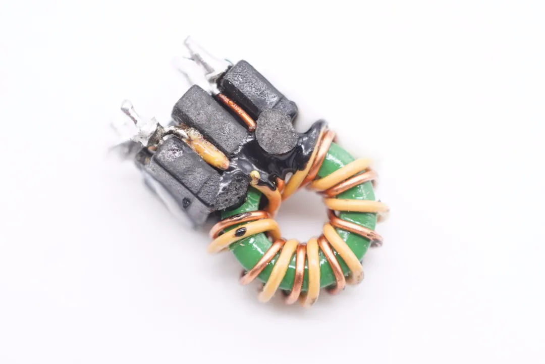
The charger input terminals, filter inductor and common mode inductor wrapped with insulating tape.
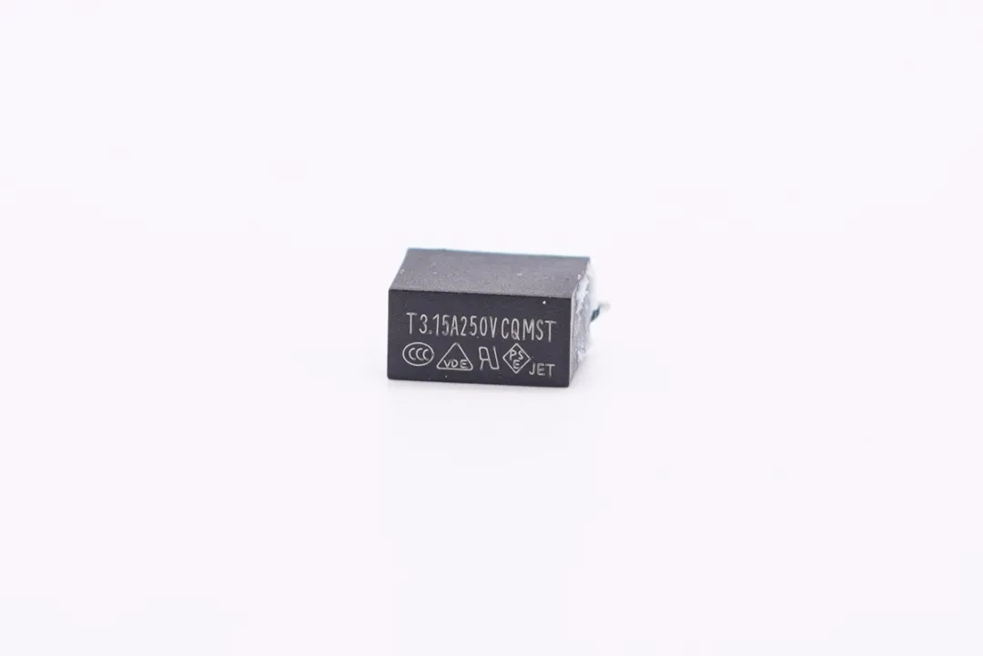
The delay fuse 3.15A 250V.
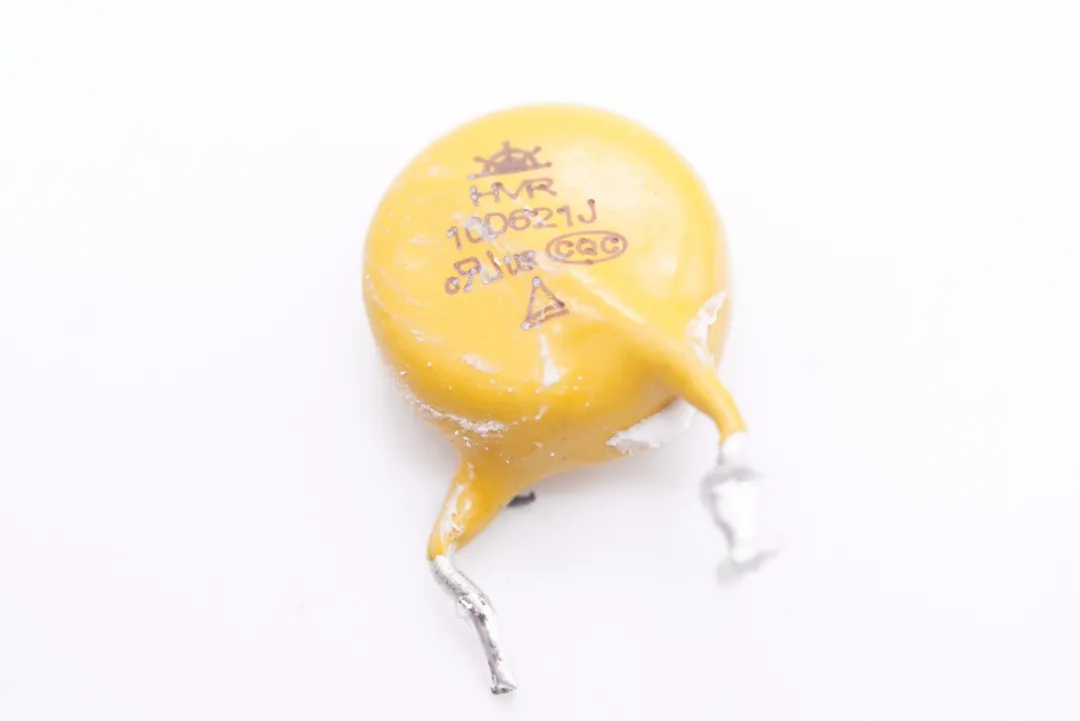
HVR10D621J varistor for input overvoltage protection.
NTC surge suppression resistors for suppressing power-on surge current.
The common-mode inductor, dual-wire winding to filter out EMI interference.
Another common-mode inductor, wrapped in insulating tape.
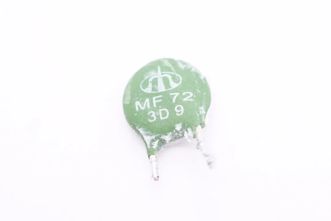
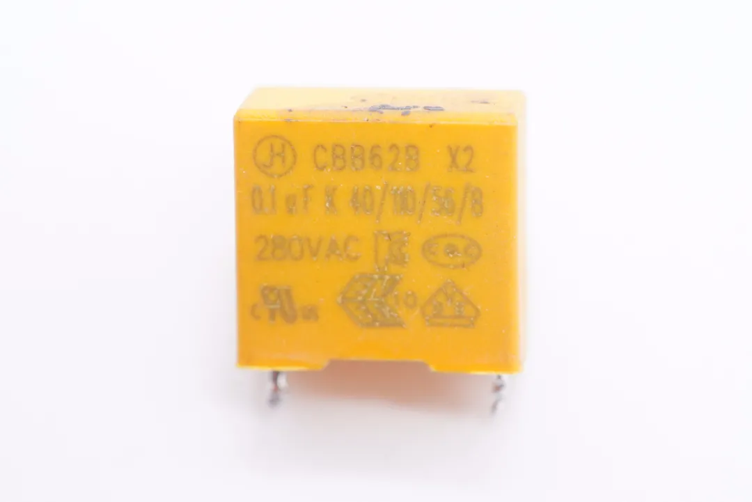
Safety regulation X capacitor 0.1μF.
Two pieces of WRMSB40M rectifier bridges at the input end for evenly distribute heat and reduce temperature rise. The WRMSB40M is from Shenzhen World Industrial Co., Ltd. The soft recovery bridge can reduce the diode junction capacitance to achieve very little harmonic oscillation through a relatively soft recovery curve and smooth turn-off characteristics.
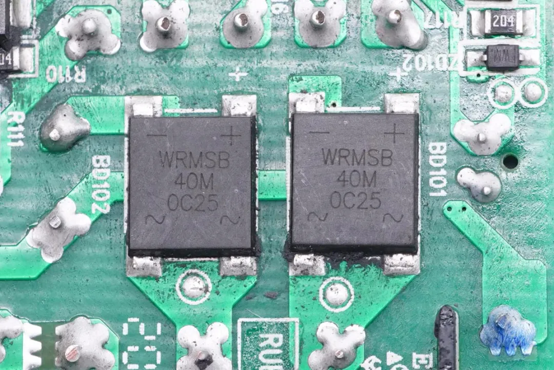
World WRMSB40M detail specification
ChargerLAB learned that Nubia 65W Three-Port GaN Fast Charger, OPPO 50W Biscuit GaN Fast Charger, HUWDER 65W GaN Charger, Amadapter 65W USB PD GaN Charger, ROCK 65W GaN Charger, Mcdodo 65W GaN Charger, Mcdodo 30W 1A1C Fast Charger are using World soft recovery bridge. The product performance has been widely recognized by customers.

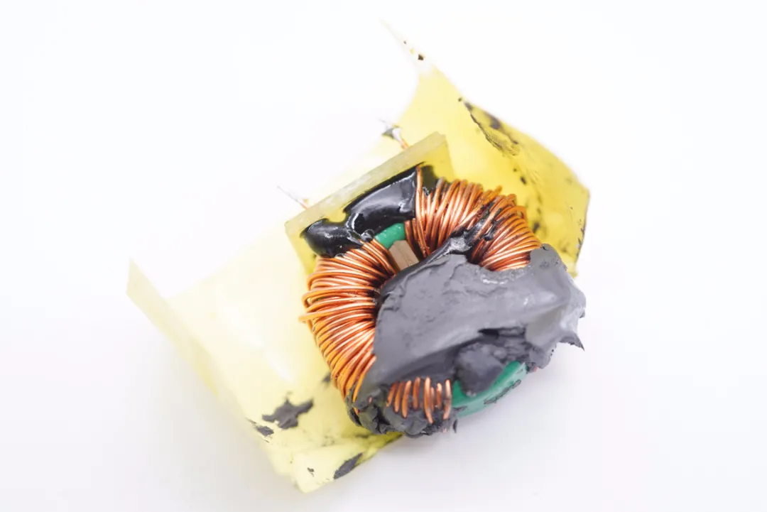
The filtered inductor.
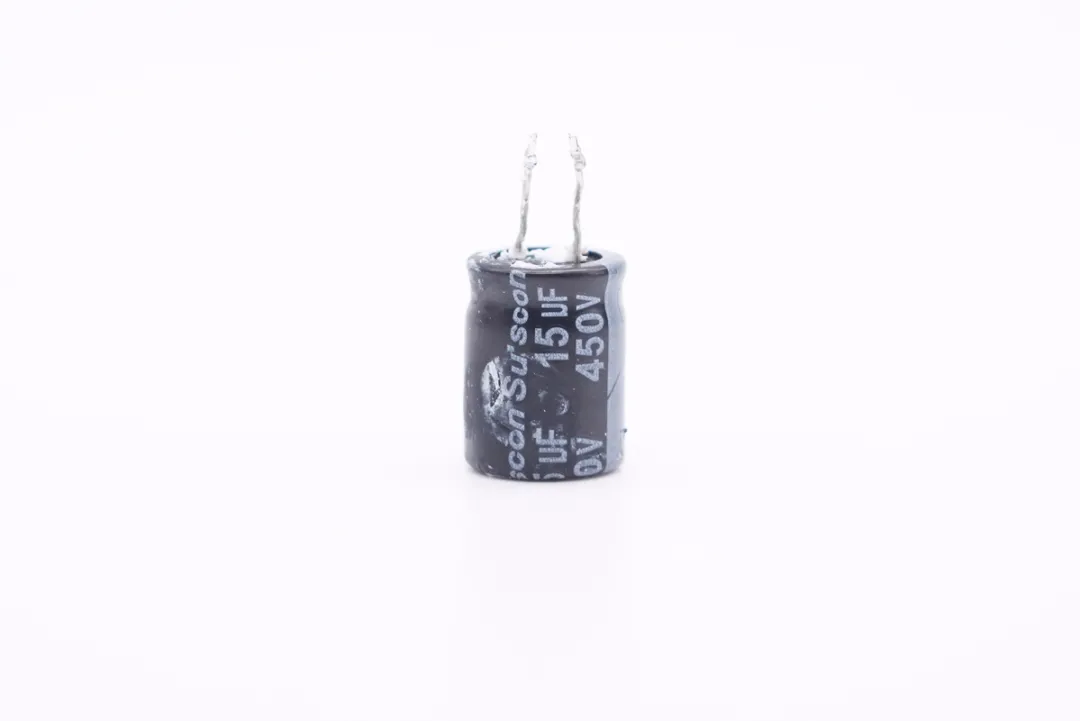
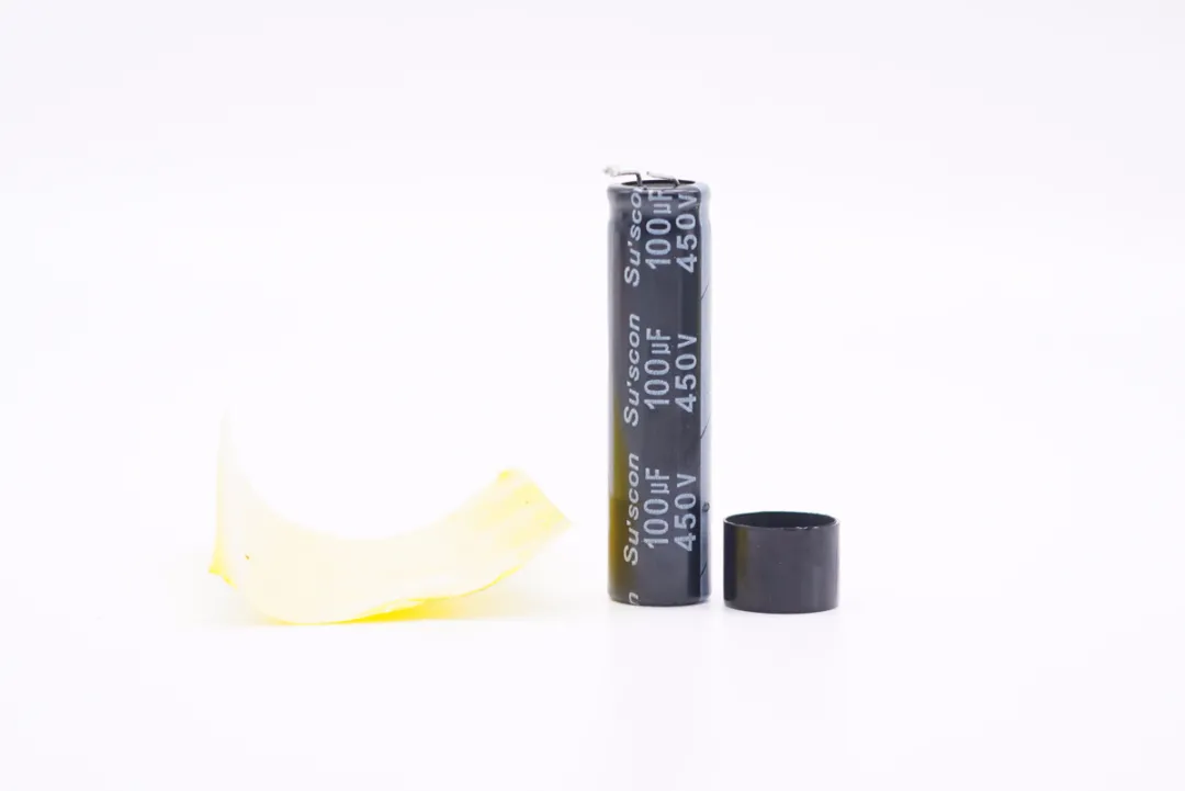
The high-voltage filter electrolytic capacitor is from Su’scon 450V 15μF.
A large-volume electrolytic capacitor is also placed horizontally on the side of the PCB board
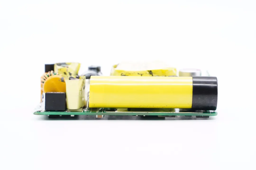
The capacitor is also from Su’scon 450V and 100μF.
The other side of the PCB board is equipped with a Y capacitor, a master control chip power supply capacitor, and a transformer.
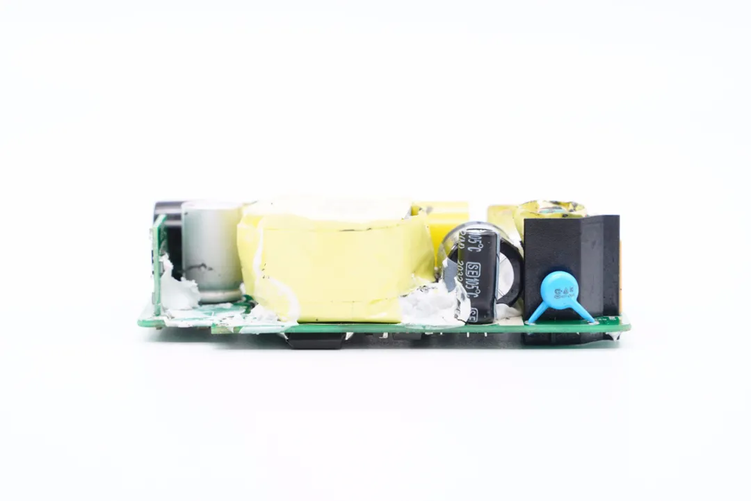
Y capacitor.

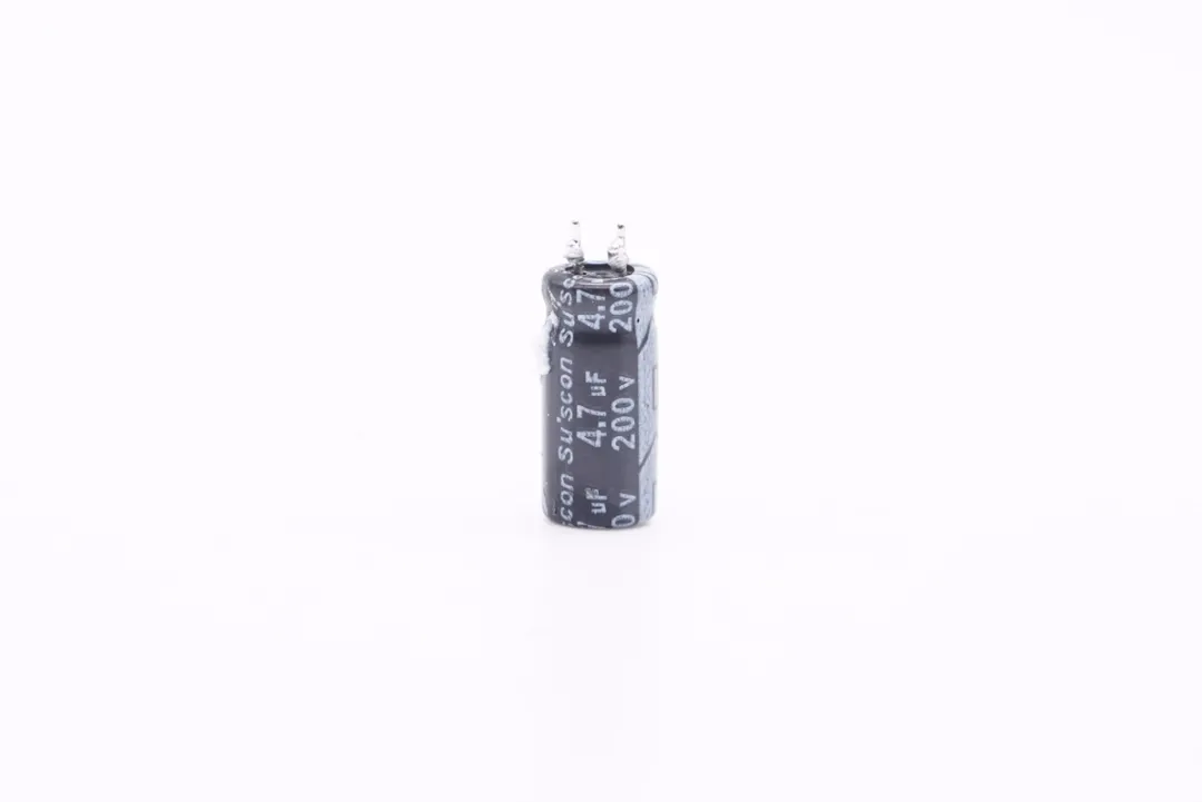
The master control chip power supply capacitor 200V 4.7μF.
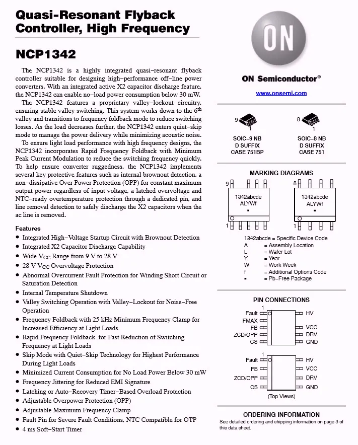
The master control chip of the charger is ON Semiconductor NCP1342
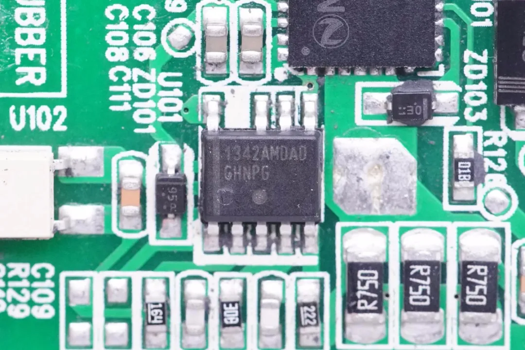
The ON Semiconductor NCP1342detail information
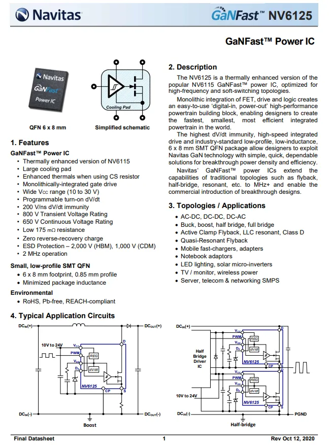
The primary side GaN power chip uses Navitas NV6125
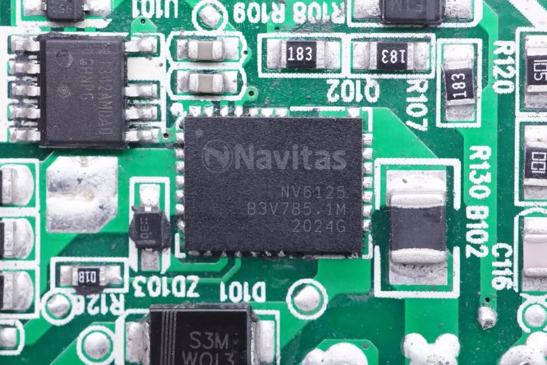
Details of Navitas Semiconductor NV6125.
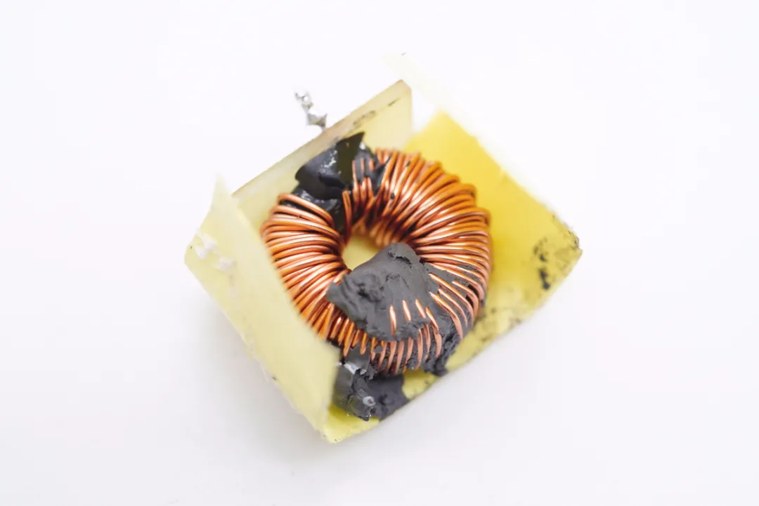
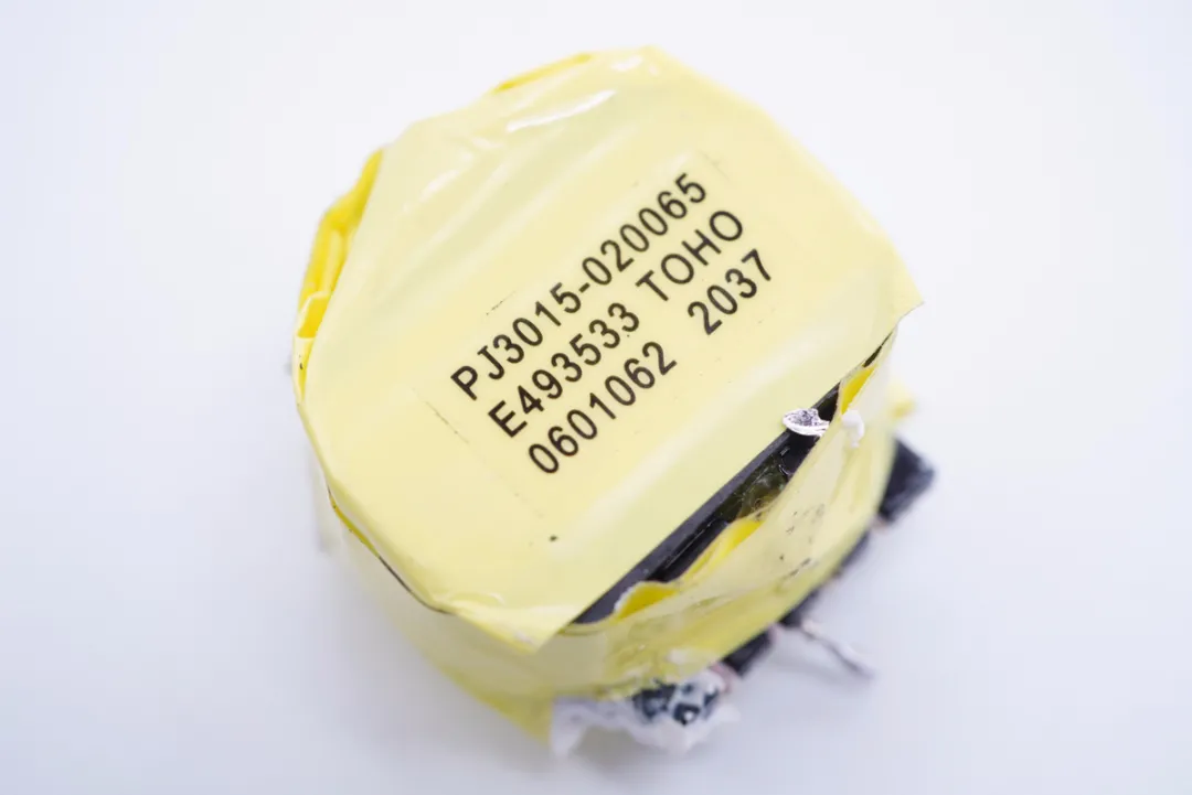
The transformer, with information labels attached.
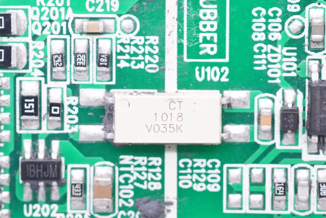
CT 1018 optocoupler for primary and secondary communication, feedback output voltage.
The chip Y capacitor for output anti-interference.
Output terminal, the protocol board is vertically welded, with output filtering solid capacitor behind it.
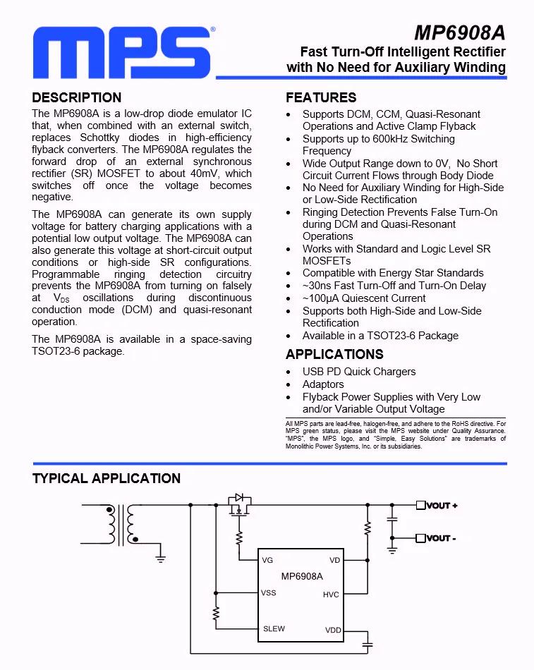
MPS Core Source Semiconductor Secondary Synchronous Rectifier Controller MP6908A
Detail specifications of MPS MP6908A.
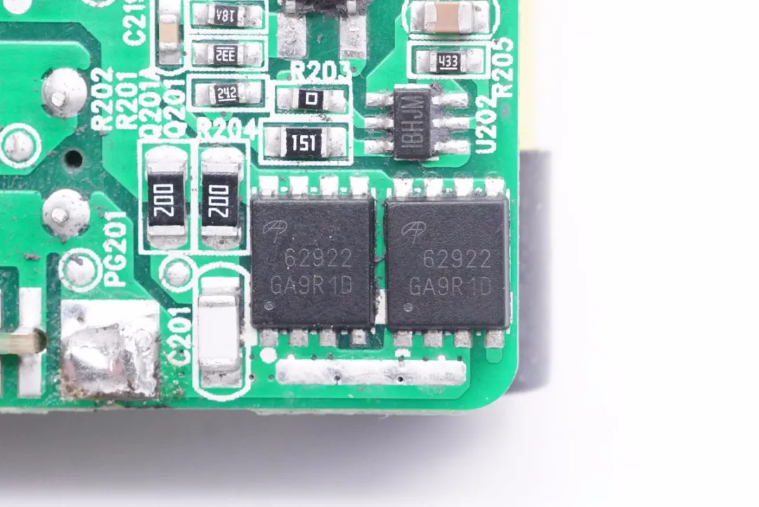
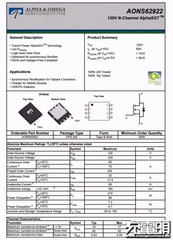
The secondary synchronous rectifier MOS uses Alpha&Omega AONS62922, NMOS, withstand voltage of 120V, and is connected in parallel.
AOS AON62922 detail specifications.
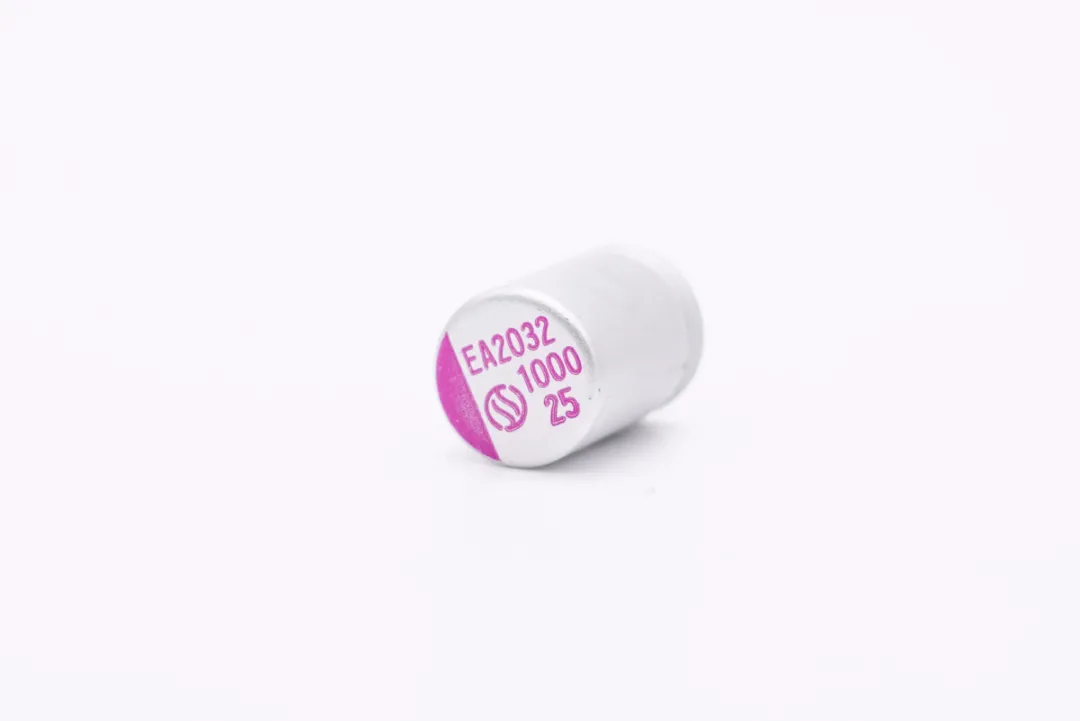
The solid capacitor for output filtering adopts the Su’scon EA series 25V 1000μF.
Remove the agreement board.
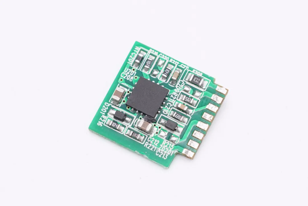
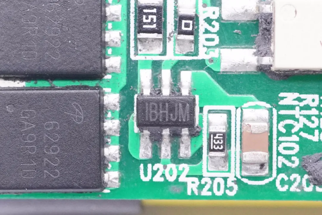
The USB PD protocol chip uses Weltrend WT6636F
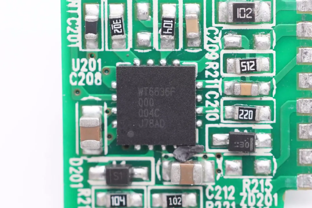
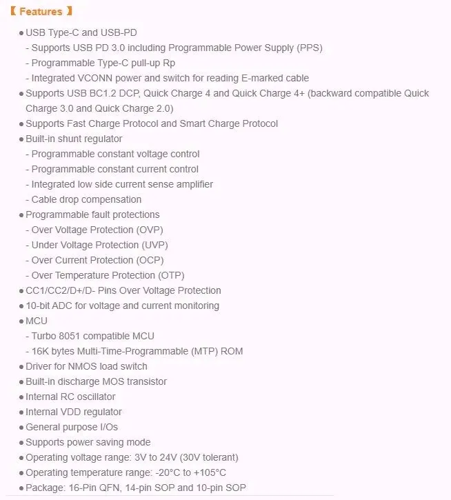
Weltrend WT6636F information.
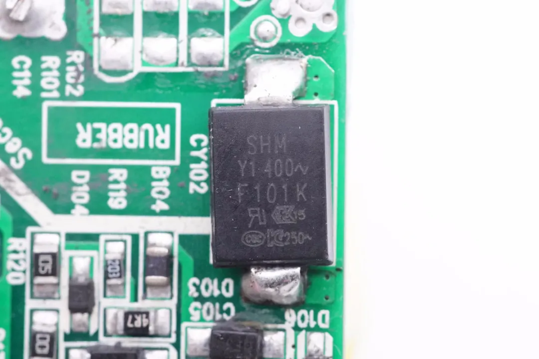
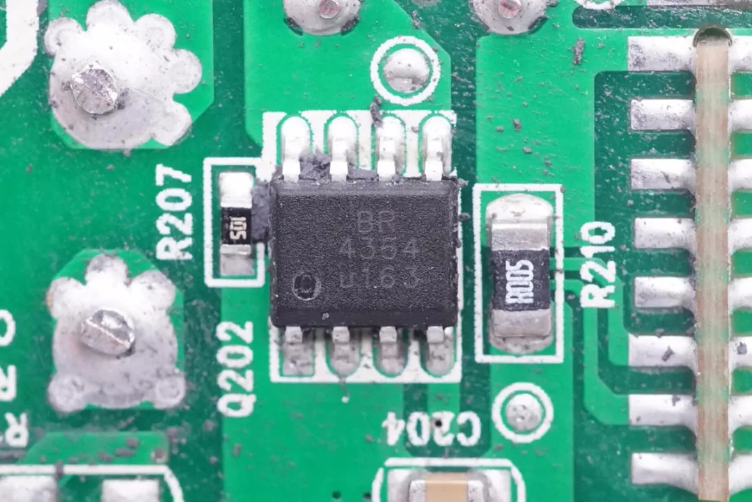
VBUS switch tube with silk screen 4354, on the right is the output current detection resistor.
That’s all for the teardown
Summary of ChargerLAB
The LG 65W PD standard fast GaN charger has a classic design and a simple style and the brick body comes with a USB-C output cable. It supports PD3.0 fast charging and has four voltage levels of 5V3A, 9V3A, 15V3A, and 20V3.25A, which can meet the daily fast charging needs of laptops.
The ChargerLAB found the charger switch power supply is composed of ON Semiconductor NCP1342 paired with Navitas NV6125 GaN power switch tube, and MPS MP6908A paired with Alpha&Omega synchronous rectifier tube. The output protocol chip uses Weltrend WT6636F certified chip, and an external thermistor is used for overheating protection. In addition, the charger uses a large-capacity capacitor for input and output filtering from Taiwan's Su’scon. The internal large area is filled with thermal conductive glue, and the overall material is solid and reliable.